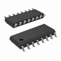
DS26C32ATM/NOPB National Semiconductor, DS26C32ATM/NOPB Datasheet

DS26C32ATM/NOPB
Specifications of DS26C32ATM/NOPB
*DS26C32ATM/NOPB
DS26C32ATM
Available stocks
Related parts for DS26C32ATM/NOPB
DS26C32ATM/NOPB Summary of contents
Page 1
... SMD or MDS. Order Number DS26C32AME/883, DS26C32AMJ/883 or DS26C32AMW/883 See NS Package E20A, J16A or W16A TRI-STATE ® registered trademark of National Semiconductor Corporation. © 2004 National Semiconductor Corporation Features n CMOS design for low power ± 0.2V sensitivity over input common mode voltage ...
Page 2
... Absolute Maximum Ratings 1) If Military/Aerospace specified devices are required, please contact the National Semiconductor Sales Office/ Distributors for availability and specifications. Supply Voltage ( Common Mode Range ( Differential Input Voltage (V ) DIFF Enable Input Voltage ( Storage Temperature Range (T STG Lead Temperature (Soldering 4 sec.) Maximum Power Dissipation at 25˚ ...
Page 3
AC Electrical Characteristics ± 10% (Note 3) CC Symbol Parameter t , Output Rise and RISE t Fall Times FALL t , Propagation Delay PLZ t ENABLE to Output PHZ t , Propagation Delay PZL t ENABLE ...
Page 4
Test and Switching Waveforms C includes load and test jig capacitance for t , and t measurements PZL PLZ S = Gnd for t and t measurements. 1 PZH PHZ FIGURE 3. TRI-STATE AC ...
Page 5
AC Test Circuit and Switching Time Waveforms FIGURE 5. Propagation Delay for “LS-Type” Load (Notes 7, 9) FIGURE 6. Enable and Disable Times for “LS-Type” Load (Notes 8, 9) Note 7: Diagram shown for ENABLE low. Note 8: S1 and ...
Page 6
Typical Performance Characteristics Differential Propagation Delay vs Temperature Differential Skew vs Temperature Output High Voltage vs Output High Current www.national.com Differential Propagation Delay 00876413 00876415 00876417 6 vs Power Supply Voltage 00876414 Differential Skew vs Power Supply Voltage 00876416 Output ...
Page 7
Typical Performance Characteristics Output Low Voltage vs Output Low Current Input Resistance vs Input Voltage Hysteresis & Differential Transition Voltage vs Temperature (Continued) 00876419 00876421 00876423 7 Output Low Voltage vs Output Low Current 00876420 Input Current vs Power Supply ...
Page 8
Typical Performance Characteristics Supply Current vs Temperature Supply Current vs Data Rate www.national.com (Continued) 00876425 00876427 8 Disabled Supply Current vs Power Supply Voltage 00876426 ...
Page 9
Physical Dimensions inches (millimeters) unless otherwise noted 20-Lead Ceramic Leadless Chip Carrier (E) Order Number DS26C32AME/883 NS Package Number E20A 16-Lead Ceramic Dual-In-Line Package (J) Order Number DS26C32AMJ/883 NS Package Number J16A 9 www.national.com ...
Page 10
Physical Dimensions www.national.com inches (millimeters) unless otherwise noted (Continued) 16-Lead Molded Small Outline Package (M) Order Number DS26C32ATM NS Package Number M16A 16-Lead Molded Dual-In-Line Package (N) Order Number DS26C32ATN NS Package Number N16E 10 ...
Page 11
... BANNED SUBSTANCE COMPLIANCE National Semiconductor certifies that the products and packing materials meet the provisions of the Customer Products Stewardship Specification (CSP-9-111C2) and the Banned Substances and Materials of Interest Specification (CSP-9-111S2) and contain no ‘‘Banned Substances’’ as defined in CSP-9-111S2. ...


