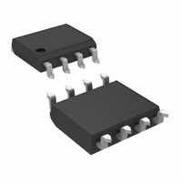
DS91C176TMAX/NOPB National Semiconductor, DS91C176TMAX/NOPB Datasheet - Page 5

DS91C176TMAX/NOPB
Manufacturer Part Number
DS91C176TMAX/NOPB
Description
IC TXRX MULTIPOINT-LVDS 8SOIC
Manufacturer
National Semiconductor
Type
Transceiverr
Datasheet
1.DS91C176TMANOPB.pdf
(14 pages)
Specifications of DS91C176TMAX/NOPB
Number Of Drivers/receivers
1/1
Protocol
LVDS
Voltage - Supply
3 V ~ 3.6 V
Mounting Type
Surface Mount
Package / Case
8-SOIC (3.9mm Width)
Number Of Elements
1
Number Of Receivers
1
Number Of Drivers
1
Input Type
CMOS/TTL
Operating Supply Voltage (typ)
3.3V
Differential Input High Threshold Voltage
150mV
Diff. Input Low Threshold Volt
50mV
Differential Output Voltage
650mV
Propagation Delay Time
7.5ns
Power Dissipation
833mW
Operating Temp Range
-40C to 85C
Operating Temperature Classification
Industrial
Mounting
Surface Mount
Pin Count
8
Lead Free Status / RoHS Status
Lead free / RoHS Compliant
Other names
DS91C176TMAX
Available stocks
Company
Part Number
Manufacturer
Quantity
Price
Company:
Part Number:
DS91C176TMAX/NOPB
Manufacturer:
TOSHIBA
Quantity:
6 264
DRIVER AC SPECIFICATION
t
t
t
t
t
t
t
t
t
t
t
f
RECEIVER AC SPECIFICATION
t
t
t
t
t
t
t
t
t
t
f
PLH
PHL
SKD1
SKD3
TLH
THL
PZH
PZL
PLZ
PHZ
JIT
MAX
PLH
PHL
SKD1
SKD3
TLH
THL
PZH
PZL
PLZ
PHZ
MAX
Switching Characteristics
Over recommended operating supply and temperature ranges unless otherwise specified.
Note 1: “Absolute Maximum Ratings” are those beyond which the safety of the device cannot be guaranteed. They are not meant to imply that the device should
be operated at these limits. The tables of “Electrical Characteristics” provide conditions for actual device operation.
Note 2: All currents into device pins are positive; all currents out of device pins are negative. All voltages are referenced to device ground unless otherwise
specified.
Note 3: All typicals are given for V
Note 4: The algebraic convention, in which the least positive (most negative) limit is designated as minimum, is used in this datasheet.
Note 5: t
the same channel.
Note 6: t
applies to devices at the same V
Note 7: Stimulus and fixture Jitter has been subtracted.
Note 8: C
Note 9: Not production tested. Guaranteed by a statistical analysis on a sample basis at the time of characterization.
Symbol
(t
(t
(t
(t
(t
(t
r
f
r
f
)
)
)
)
sk(p)
sk(p)
SKD1
SKD3
L
)
)
includes fixture capacitance and C
, |t
, Part-to-Part Skew, is defined as the difference between the minimum and maximum specified differential propagation delays. This specification
PLHD
Differential Propagation Delay Low to High
Differential Propagation Delay High to Low
Pulse Skew |t
Part-to-Part Skew
Rise Time
Fall Time
Enable Time (Z to Active High)
Enable Time (Z to Active Low )
Disable Time (Active Low to Z)
Disable Time (Active High to Z)
Random Jitter, RJ
Maximum Data Rate
Propagation Delay Low to High
Propagation Delay High to Low
Pulse Skew |t
Part-to-Part Skew
Rise Time
Fall Time
Enable Time (Z to Active High)
Enable Time (Z to Active Low)
Disable Time (Active Low to Z)
Disable Time (Active High to Z)
Maximum Data Rate
− t
PHLD
|, is the magnitude difference in differential propagation delay time between the positive going edge and the negative going edge of
(Note
(Note
(Note
(Note
CC
CC
PLHD
PLHD
and within 5°C of each other within the operating temperature range.
9)
9)
= 3.3V and T
Parameter
9)
9)
(Note
(Note
− t
− t
(Note
PHLD
PHLD
D
includes probe capacitance.
6,
6,
9)
|
|
A
(Note
(Note
Note
Note
= 25°C.
9)
9)
5,
5,
Note
Note
9)
9)
R
C
Figure 7
R
C
Figure 9
100 MHz Clock Pattern
C
Figures 11, 12 and
R
Figure 14
L
D
L
D
L
L
= 50Ω, C
= 50Ω, C
= 15 pF
= 500Ω, C
5
= 0.5 pF
= 0.5 pF
and
and
and
L
L
Conditions
Figure 8
Figure 10
L
= 5 pF,
= 5 pF,
Figure 15
= 15 pF
Figure 13
(Note
(Note
7)
3,
Note
Min
200
200
1.3
1.3
1.0
1.0
2.0
2.0
0.5
0.5
8)
Typ
300
3.4
3.1
1.8
1.8
2.5
4.7
5.3
0.6
1.2
1.2
www.national.com
Max
420
5.0
5.0
1.3
3.0
3.0
5.5
7.5
7.5
1.7
1.3
2.5
2.5
10
10
10
10
8
8
8
8
psrms
Units
Mbps
Mbps
ns
ns
ps
ns
ns
ns
ns
ns
ns
ns
ns
ns
ns
ns
ns
ns
ns
ns
ns
ns


