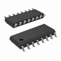
LMS202ECM/NOPB National Semiconductor, LMS202ECM/NOPB Datasheet - Page 4

LMS202ECM/NOPB
Manufacturer Part Number
LMS202ECM/NOPB
Description
TXRX DUAL 5V TIA/EIA-232 16-SOIC
Manufacturer
National Semiconductor
Type
Transceiverr
Datasheet
1.LMS202ECMXNOPB.pdf
(6 pages)
Specifications of LMS202ECM/NOPB
Number Of Drivers/receivers
2/2
Protocol
RS232
Voltage - Supply
4.5 V ~ 5.5 V
Mounting Type
Surface Mount
Package / Case
16-SOIC (3.9mm Width)
Lead Free Status / RoHS Status
Lead free / RoHS Compliant
Other names
LMS202ECM
www.national.com
T
T
V
DPLH
DPHL
SLEW
Symbol
Note 1: Absolute Maximum Ratings indicate limits beyond which damage to the device may occur. Operating Ratings indicate conditions for which the device is
intended to be functional, but specific performance is not guaranteed. For guaranteed specifications and the test conditions, see the Electrical Characteristics.
Note 2: Human Body Model, 1.5kΩ in series with 100pF
Note 3: The maximum power dissipation is a function of T
(MAX)
Note 4: Typical Values represent the most likely parametric norm.
Note 5: All limits are guaranteed by testing or statistical analysis
Note 6: Machine model, 0Ω in series with 200pF
Typical Characteristics
Application Information
CAPACITOR SELECTION
The recommended capacitors are 0.1μF. However, larger ca-
pacitors for the charge pump may be used to minimized
ripples on V+ and V− pins.
POWER SUPPLY DECOUPLING
In some applications that are sensitive to power supply noise
from the charge pump, place a decoupling capacitor, Cbp,
Transmitter Output High Voltage vs. Load Capacitance
− T
A
)/ θ
JA.
Transmitter Propagation
Delay
Transition Region Slew Rate T
All numbers apply for packages soldered directly onto a PC board.
Parameter
200629 Version 5 Revision 2
R
All transmitters loaded
C
Measured from +3V to −3V or vice versa
A
L
L
= 3kΩ, C
= 25°C, V
= 50pF to 1000pF, R
J(MAX),
θ
20062902
JA,
L
S
= 2500pF
and T
= 5V
Conditions
A.
The maximum allowable power dissipation at any ambient temperature is P
Print Date/Time: 2010/07/12 17:35:02
4
L
= 3kΩ to 7kΩ
from V
size as the charge pump capacitors (C1 − C4).
CHARGED PUMP
The dual internal charged-pump provides the ±10V to the to
transmitters. Using capacitor C1, the charge pump converts
+5V to +10V then stores the +10V in capacitor C3. The charge
pump uses capacitor C2 to invert the +10V to −10V. The −10V
is then stored in capacitor C4.
Transmitter Slew Rate vs. Load Capacitance
S
to GND. Use at least a 0.1µF capacitor or the same
(Note
Min
3
5)
Typ
2.4
6
(Note
Max
30
5)
20062903
Units
D
V/μs
μs
= (T
J


