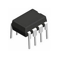
ADC0832CCN National Semiconductor, ADC0832CCN Datasheet - Page 18

ADC0832CCN
Manufacturer Part Number
ADC0832CCN
Description
A/D Converter (A-D) IC
Manufacturer
National Semiconductor
Datasheet
1.ADC0832CCN.pdf
(33 pages)
Specifications of ADC0832CCN
No. Of Pins
8
Peak Reflow Compatible (260 C)
No
Leaded Process Compatible
No
Package / Case
8-DIP
Rohs Compliant
No
Number Of Elements
1
Resolution
8Bit
Architecture
SAR
Sample Rate
31KSPS
Input Polarity
Unipolar
Input Type
Voltage
Rated Input Volt
5V
Differential Input
Yes
Power Supply Requirement
Single
Single Supply Voltage (typ)
5V
Single Supply Voltage (min)
4.5V
Single Supply Voltage (max)
6.3V
Dual Supply Voltage (typ)
Not RequiredV
Dual Supply Voltage (min)
Not RequiredV
Dual Supply Voltage (max)
Not RequiredV
Power Dissipation
800mW
Operating Temp Range
0C to 70C
Operating Temperature Classification
Commercial
Mounting
Through Hole
Pin Count
8
Package Type
PDIP
Lead Free Status / Rohs Status
Not Compliant
Available stocks
Company
Part Number
Manufacturer
Quantity
Price
Company:
Part Number:
ADC0832CCN
Manufacturer:
NS
Quantity:
6 000
Company:
Part Number:
ADC0832CCN
Manufacturer:
NS
Quantity:
520
Company:
Part Number:
ADC0832CCN
Manufacturer:
NS
Quantity:
6 000
Part Number:
ADC0832CCN
Manufacturer:
NS/国半
Quantity:
20 000
Company:
Part Number:
ADC0832CCN/NOPB
Manufacturer:
STMicroelectronics
Quantity:
2 000
www.national.com
Functional Description
resistance of the analog signal source. Bypass capacitors
should not be used if the source resistance is greater than 1
kΩ.
This source resistance limitation is important with regard to
the DC leakage currents of input multiplexer as well. The
worst-case leakage current of
create a 1 mV input error with a 1 kΩ source resistance. An
op amp RC active low pass filter can provide both imped-
ance buffering and noise filtering should a high impedance
signal source be required.
5.0 Optional Adjustments
5.1 Zero Error
The zero of the A/D does not require adjustment. If the
minimum analog input voltage value, V
a zero offset can be done. The converter can be made to
output 0000 0000 digital code for this minimum input voltage
by biasing any V
utilizes the differential mode operation of the A/D.
The zero error of the A/D converter relates to the location of
the first riser of the transfer function and can be measured by
grounding the V
positive voltage to the V
ence between the actual DC input voltage which is neces-
sary to just cause an output digital code transition from 0000
0000 to 0000 0001 and the ideal
mV for V
5.2 Full-Scale
The full-scale adjustment can be made by applying a differ-
ential input voltage which is 1
analog full-scale voltage range and then adjusting the mag-
nitude of the V
digital output code which is just changing from 1111 1110 to
1111 1111.
5.3 Adjusting for an Arbitrary Analog Input Voltage
Range
If the analog zero voltage of the A/D is shifted away from
ground (for example, to accommodate an analog input signal
which does not go to ground), this new zero reference
should be properly adjusted first. A V
equals this desired zero reference plus
LSB is calculated for the desired analog span, using 1 LSB=
analog span/256) is applied to selected “+” input and the
zero reference voltage at the corresponding “−” input should
then be adjusted to just obtain the 00
transition.
The full-scale adjustment should be made [with the proper
V
input which is given by:
IN
(−) voltage applied] by forcing a voltage to the V
REF
=5.000 V
REF
IN
(−) input and applying a small magnitude
IN
input (or V
(−) input at this V
DC
).
IN
(+) input. Zero error is the differ-
1
⁄
2
±
CC
1 µA over temperature will
LSB down from the desired
1
⁄
2
for the ADC0832) for a
LSB value (
IN(MIN)
IN
HEX
1
(Continued)
IN(MIN)
⁄
(+) voltage which
2
LSB (where the
to 01
, is not ground
1
value. This
⁄
2
HEX
LSB=9.8
code
IN
(+)
18
where:
and
The V
change from FE
ment procedure.
6.0 Power Supply
A unique feature of the ADC0838 and ADC0834 is the inclu-
sion of a zener diode connected from the V
ground which also connects to the V
actual converter supply) through a silicon diode, as shown in
Figure 3. (Note 3)
This zener is intended for use as a shunt voltage regulator to
eliminate the need for any additional regulating components.
This is most desirable if the converter is to be remotely
located from the system power source.Figure 4 and Figure 5
illustrate two useful applications of this on-board zener when
an external transistor can be afforded.
An important use of the interconnecting diode between V
and V
is used as a rectifier to allow the V
to be derived from the clock. The low current requirements of
the A/D and the relatively high clock frequencies used (typi-
cally in the range of 10k–400 kHz) allows using the small
value filter capacitor shown to keep the ripple on the V
to well under
also be used in this mode. This requires a clock voltage
swing which is in excess of V
needed, either built into the clock generator or a resistor can
be used from the CLK pin to the V
V
V
FIGURE 3. An On-Chip Shunt Regulator Diode
MAX
MIN
REF
CC
is shown in Figure 6 and Figure 7. Here, this diode
= the low end (the offset zero) of the analog
(or V
= the high end of the analog input range
range.
(Both are ground referenced.)
1
CC
⁄
4
HEX
of an LSB. The shunt zener regulator can
) voltage is then adjusted to provide a code
to FF
HEX
Z
. A current limit for the zener is
. This completes the adjust-
CC
+
CC
supply for the converter
pin.
terminal (which is the
00558311
+
terminal to
CC
line
+


