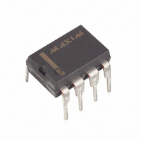
MAX3430CPA+ Maxim Integrated Products, MAX3430CPA+ Datasheet - Page 10

MAX3430CPA+
Manufacturer Part Number
MAX3430CPA+
Description
IC TXRX RS-485 3.3V 8-DIP
Manufacturer
Maxim Integrated Products
Type
Transceiverr
Datasheet
1.MAX3430ESA.pdf
(13 pages)
Specifications of MAX3430CPA+
Number Of Drivers/receivers
1/1
Protocol
RS485
Voltage - Supply
3 V ~ 3.6 V
Mounting Type
Through Hole
Package / Case
8-DIP (0.300", 7.62mm)
Data Rate
250Kbps
Supply Voltage Range
3V To 3.6V
Logic Case Style
DIP
No. Of Pins
8
Operating Temperature Range
0°C To +70°C
Data Rate Max
250Kbps
Driver Case Style
DIP
Rohs Compliant
Yes
Lead Free Status / RoHS Status
Lead free / RoHS Compliant
stage, provides immediate protection against short cir-
cuits over the whole common-mode voltage range. The
second, a thermal shutdown circuit, forces the driver
outputs into a high-impedance state if the die tempera-
ture exceeds +160°C. Normal operation resumes when
the die temperature cools by +140°C, resulting in a
pulsed output during continuous short-circuit conditions.
±80V Fault-Protected, Fail-Safe,
1/4-Unit Load, +3.3V RS-485 Transceiver
Figure 9. Simplified Structure of the Driver Enable Pin (DE)
Figure 10. Typical RS-485 Network
10
DE
TIMER
V
______________________________________________________________________________________
CC
5.6kΩ
RO
RE
DE
DI
TIMER
M1
100µA
15µs
D
MAX3430
R
2mA
M2
B
A
120Ω
B
DI
D
(HOT SWAP)
A
DE
DE
RO
R
RE
Inserting circuit boards into a hot, or powered backplane
may cause voltage transients on DE, RE, and receiver
inputs A and B that can lead to data errors. For example,
upon initial circuit board insertion, the processor under-
goes a power-up sequence. During this period, the high-
impedance state of the output drivers makes them
unable to drive the MAX3430 enable inputs to a defined
logic level. Meanwhile, leakage currents of up to 10µA
from the high-impedance output, or capacitively coupled
noise from V
an incorrect logic state. To prevent such a condition from
occurring, the MAX3430 features hot-swap input circuitry
on DE to safeguard against unwanted driver activation
during hot-swap situations. When V
pulldown circuit holds DE low for at least 10µs, and until
the current into DE exceeds 200µA. After the initial
power-up sequence, the pulldown circuit becomes
transparent, resetting the hot-swap tolerable input.
At the driver enable input (DE), there are two NMOS
devices, M1 and M2
0, an internal 15µs timer turns on M2 and sets the SR
latch, which also turns on M1. Transistors M2, a 2mA
current sink, and M1, a 100µA current sink, pull DE to
GND through a 5.6kΩ resistor. M2 pulls DE to the dis-
abled state against an external parasitic capacitance
up to 100pF that may drive DE high. After 15µs, the
timer deactivates M2 while M1 remains on, holding DE
low against three-state leakage currents that may drive
DE high. M1 remains on until an external current source
overcomes the required input current. At this time, the
SR latch resets M1 and turns off. When M1 turns off, DE
reverts to a standard, high-impedance CMOS input.
Whenever V
B
DI
D
A
CC
DE
CC
drops below 1V, the input is reset.
or GND, could cause an input to drift to
120Ω
RO
R
RE
(Figure
B
A
Hot-Swap Capability
Hot-Swap Input Circuitry
9). When V
R
CC
D
Hot-Swap Inputs
rises, an internal
CC
RO
DE
DI
RE
ramps from


