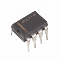
MAX3430CPA+ Maxim Integrated Products, MAX3430CPA+ Datasheet - Page 9

MAX3430CPA+
Manufacturer Part Number
MAX3430CPA+
Description
IC TXRX RS-485 3.3V 8-DIP
Manufacturer
Maxim Integrated Products
Type
Transceiverr
Datasheet
1.MAX3430ESA.pdf
(13 pages)
Specifications of MAX3430CPA+
Number Of Drivers/receivers
1/1
Protocol
RS485
Voltage - Supply
3 V ~ 3.6 V
Mounting Type
Through Hole
Package / Case
8-DIP (0.300", 7.62mm)
Data Rate
250Kbps
Supply Voltage Range
3V To 3.6V
Logic Case Style
DIP
No. Of Pins
8
Operating Temperature Range
0°C To +70°C
Data Rate Max
250Kbps
Driver Case Style
DIP
Rohs Compliant
Yes
Lead Free Status / RoHS Status
Lead free / RoHS Compliant
The driver accepts a single-ended, logic-level input
(DI) and transfers it to a differential, RS-485 level output
(A and B). Driving DE high enables the driver, while
pulling DE low places the driver outputs (A and B) into
a high-impedance state.
The receiver accepts a differential, RS-485 level input
(A and B), and transfers it to a single-ended, logic-level
output (RO). Pulling RE low enables the receiver, while
driving RE high and DE low places the receiver inputs
(A and B) into a high-impedance state.
Force DE low and RE high to shut down the MAX3430. A
time delay of 1µs prevents the device from accidentally
entering shutdown due to logic skews when switching
between transmit and receive modes. Holding DE low
and RE high for at least 1ms guarantees that the
MAX3430 enters shutdown. In shutdown, the device
consumes 100µA supply current.
The driver outputs/receiver inputs of RS-485 devices in
industrial network applications often experience voltage
faults resulting from transients that exceed the -7V to
+12V range specified in the EIA/TIA-485 standard. In
these applications, ordinary RS-485 devices (typical
absolute maximum ratings -8V to +12.5V) require costly
external protection devices. To reduce system com-
plexity and the need for external protection, the driver
outputs/receiver inputs of the MAX3430 withstand volt-
age faults of up to ±80V with respect to ground without
damage (see the Absolute Maximum Ratings section,
Note 1). Protection is guaranteed regardless of whether
the device is active, shut down, or without power.
Figure 8a. Human Body ESD Test Model
VOLTAGE
SOURCE
HIGH-
DC
CHARGE-CURRENT-
LIMIT RESISTOR
1MΩ
R
C
100pF
_______________________________________________________________________________________
C s
Detailed Description
1/4-Unit Load, +3.3V RS-485 Transceiver
STORAGE
CAPACITOR
1.5kΩ
RESISTANCE
DISCHARGE
R
Low-Power Shutdown
±80V Fault Protection
D
±80V Fault-Protected, Fail-Safe,
Receiver
DEVICE
UNDER
TEST
Driver
The MAX3430 uses a -50mV to -200mV differential
input threshold to ensure true fail-safe receiver inputs.
This threshold guarantees the receiver outputs a logic
high for shorted, open, or idle data lines. The -50mV to
-200mV threshold complies with the ±200mV threshold
EIA/TIA-485 standard.
As with all Maxim devices, ESD-protection structures
are incorporated on all pins to protect against ESD
encountered during handling and assembly. The
MAX3430 receiver inputs/driver outputs (A, B) have
extra protection against static electricity found in nor-
mal operation. Maxim’s engineers have developed
state-of-the-art structures to protect these pins against
±12kV ESD without damage. After an ESD event, the
MAX3430 continues working without latchup.
ESD protection can be tested in several ways. The
receiver inputs are characterized for protection up to
±12kV using the Human Body Model.
ESD performance depends on a number of conditions.
Contact Maxim for a reliability report that documents
test setup, methodology, and results.
Figure 8a shows the Human Body Model, and Figure
8b shows the current waveform it generates when dis-
charged into a low impedance. This model consists of
a 100pF capacitor charged to the ESD voltage of inter-
est, which is then discharged into the device through a
1.5kΩ resistor.
Two mechanisms prevent excessive output current and
power dissipation caused by faults or bus contention.
The first, a foldback current limit on the driver output
Figure 8b. Human Body Model Current Waveform
AMPERES
I
P
36.8%
100%
90%
10%
0
0
t
RL
Driver Output Protection
CURRENT WAVEFORM
TIME
±12kV ESD Protection
t
DL
ESD Test Conditions
I r
Human Body Model
PEAK-TO-PEAK RINGING
(NOT DRAWN TO SCALE)
True Fail-Safe
9


