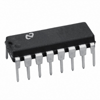
DP8392CN-1 National Semiconductor, DP8392CN-1 Datasheet - Page 6

DP8392CN-1
Manufacturer Part Number
DP8392CN-1
Description
IC TXRX COAX INTERFACE 16-DIP
Manufacturer
National Semiconductor
Type
Transceiverr
Datasheet
1.DP8392CN-1.pdf
(10 pages)
Specifications of DP8392CN-1
Protocol
IEEE 802
Voltage - Supply
9V
Mounting Type
Through Hole
Package / Case
16-DIP (0.300", 7.62mm)
Lead Free Status / RoHS Status
Contains lead / RoHS non-compliant
Number Of Drivers/receivers
-
Other names
*DP8392CN-1
Available stocks
Company
Part Number
Manufacturer
Quantity
Price
Part Number:
DP8392CN-1
Manufacturer:
NS/国半
Quantity:
20 000
6 0 Absolute Maximum Ratings
Supply Voltage (V
Package Power Rating at 25 C
Input Voltage
Storage Temperature
Lead Temp (Soldering 10 seconds)
7 0 Electrical Characteristics
8 0 Switching Characteristics
Note 1 Absolute maximum ratings are those values beyond which the safety of the device cannot be guaranteed They are not meant to imply that the device
should be operated at these limits
Note 2 All currents into device pins are positive all currents out of device pins are negative All voltages referenced to ground unless otherwise specified
Note 3 All typicals are given for V
Symbol
t
t
t
t
t
t
t
t
t
t
t
t
t
t
t
f
t
t
t
t
t
For actual power dissipation of the device please refer to section 7 0
Symbol
I
I
I
I
I
V
V
V
V
V
C
R
R
RON
Rd
Rr
Rf
RJ
TST
Td
Tr
Tf
TM
TS
TON
TOFF
CON
COFF
CD
CP
HON
HW
JA
JR
EE1
EE2
RXI
TDC
TAC
(PC Board Mounted)
Derate linearly at the rate of 28 6 mW C
CD
OD
OC
OB
TS
X
RXI
TXO
Receiver startup delay (RXI to RX
Receiver propagation delay (RXI to RX
Differential outputs rise time (RX
Differential outputs fall time (RX
Receiver
Transmitter startup delay (TX
Transmitter propagation delay (TX
Transmitter rise time
Transmitter fall time
t
Transmitter skew (TXO)
Transmit turn-on pulse width at V
Transmit turn-off pulse width at V
Collision turn-on delay
Collision turn-off delay
Collision frequency (CD
Collision pulse width (CD
CD Heartbeat delay (TX
CD Heartbeat duration (CD
Jabber activation delay (TX
Jabber reset unjab time (TX
Tr
EE
Supply current out of V
Supply current out of V
Receive input bias current (RXI)
Transmit output dc current level (TXO)
Transmit output ac current level (TXO)
Collision threshold (Receive mode)
Differential output voltage (RX
Common mode output voltage (RX
Diff output voltage imbalance (RX
Transmitter squelch threshold (TX
Input capacitance (RXI)
Shunt resistance non transmitting (RXI)
Shunt resistance transmitting (TXO)
and t
)
Tf
mismatch
EE
cable total jitter
e b
9V and T
Parameter
Parameter
90% to 10% (TXO)
10% to 90% (TXO)
g
g
EE
EE
g
)
A
to CD
)
g
g
e
g
pin non transmitting
pin transmitting
)
b
g
25 C
See Section 5
to TXO and CD
to TXO and CD
65 to 150 C
g
to TXO)
g
g
g
V
TS
TS
3 5 Watts
0 to
g
V
g
EE
)
CD
(Note 1)
EE
CD
)
CD
(TX
g
(TX
g
g
to TXO)
b
b
e b
260 C
)
g
e b
g
g
g
CD
g
g
12V
12V
CD
)
)
)
)
)
)
9V
g
g
9V
)
g
)
g
g
g
6
)
)
5% T
5% T
Recommended Operating
Conditions
Supply Voltage (V
Ambient Temperature
If Military Aerospace specified devices are required
please contact the National Semiconductor Sales
Office Distributors for availability and specifications
A
A
5
5
5
5
6
6
6
6
6
6
7
7
7
7
8
8
9
9
e
e
Fig
10
b
g
b
b
0 to 70 C (Notes 2
g
Min
100
b
0 to 70 C (Note 3)
11
11
11
11
11
11
11
11
11
11
11
11
11
11
11
11
11
11
37
1 45
550
175
1 5
28
2
EE
Min
250
8 0
0 6
0 5
35
20
)
b
b
b
b
b
Typ
1 2
41
10
1 53
125
225
2 0
85
3)
g
Typ
250
500
g
0 5
1 0
15
25
25
25
20
29
4
4
4
1
0 5
7
2
g
b
b
b
b
b
a
Max
I
g
TDC
1200
45
1 58
130
180
300
2 5
40
25
Max
12 5
750
1 6
1 5
50
50
20
70
60
b
0 to 70 C
9v
Units
Units
mA
mA
mA
mA
mV
mV
mV
K
K
g
MHz
pF
bits
bits
bits
bits
ms
ms
V
V
ns
ns
ns
ns
ns
ns
ns
ns
ns
ns
ns
ns
A
5%
s
s


