DSV14196WM National Semiconductor, DSV14196WM Datasheet
DSV14196WM
Specifications of DSV14196WM
Available stocks


Related parts for DSV14196WM

DSV14196WM Summary of contents
Page 1
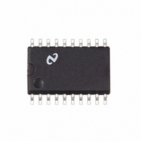
... The DSV14196/DSV14196T provides a pe- ripheral side one-chip solution for the common 9-pin serial RS-232 interface between data terminals and data commu- nications equipment. Connection Diagram SOP Order Number DSV14196WM,DSV14196TWM See NS Package Number M20B LapLink ® registered trademark of Travelling Software. © 2004 National Semiconductor Corporation Features n Conforms to EIA/TIA-232-E and ITU-T V ...
Page 2
... Absolute Maximum Ratings If Military/Aerospace specified devices are required, please contact the National Semiconductor Sales Office/ Distributors for availability and specifications. Supply Voltage ( Supply Voltage (V ) − Supply Voltage (V ) Driver Input Voltage Driver Output Voltage (Power Off) Receiver Input Voltage Receiver Output Voltage (R ...
Page 3
Electrical Characteristics DSV14196 (Continued) Over recommended operating supply and temperature ranges unless otherwise specified Symbol Parameter RECEIVER CHARACTERISTICS V Input High Threshold TH (Recognized as a High Signal) V Input Low Threshold TL (Recognized as a Low Signal) R Input ...
Page 4
Electrical Characteristics DSV14196T (Continued) Over recommended operating supply and temperature ranges unless otherwise specified Symbol Parameter RECEIVER CHARACTERISTICS V Input High Threshold TH (Recognized as a High Signal) V Input Low Threshold TL (Recognized as a Low Signal) R Input ...
Page 5
Parameter Measurement Information FIGURE 1. Driver Propagation Delay and Transition Time Test Circuit (Note 5) FIGURE 2. Driver Propagation Delay and Transition Time Waveforms Slew Rate (SR) = 6V/(t FIGURE 3. Receiver Propagation Delay and Transition Time Test Circuit (Note ...
Page 6
Applications Information In a typical Data Terminal Equipment (DTE) to Data Circuit- Terminating Equipment (DCE) 9-pin de-facto interface imple- mentation, 2 data lines and 6 control lines are required. The data lines are TXD and RXD. The control lines are ...
Page 7
Typical Performance Characteristics Driver Output Slew Rate between +3V and −3V vs Load Capacitance Conditions 3.3V kΩ kHz Square Wave Driver Output Current vs Output Voltage = 25˚ Driver ...
Page 8
... National does not assume any responsibility for use of any circuitry described, no circuit patent licenses are implied and National reserves the right at any time without notice to change said circuitry and specifications. inches (millimeters) unless otherwise noted Order Number DSV14196WM NS Package Number M20B 2 ...