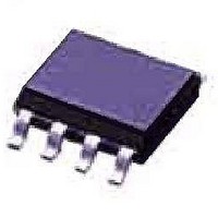
ATTINY12-8SU Atmel, ATTINY12-8SU Datasheet - Page 13

ATTINY12-8SU
Manufacturer Part Number
ATTINY12-8SU
Description
Microcontrollers (MCU) AVR 1K FLASH 64B EE 5V 8MHZ
Manufacturer
Atmel
Datasheet
1.ATTINY12-8SU.pdf
(94 pages)
Specifications of ATTINY12-8SU
Processor Series
ATTINY1x
Core
AVR8
Data Bus Width
8 bit
Program Memory Type
Flash
Program Memory Size
1 KB
Maximum Clock Frequency
8 MHz
Number Of Programmable I/os
6
Number Of Timers
1
Maximum Operating Temperature
+ 85 C
Mounting Style
SMD/SMT
Package / Case
SOIC
3rd Party Development Tools
EWAVR, EWAVR-BL
Development Tools By Supplier
ATAVRDRAGON, ATSTK500
Minimum Operating Temperature
- 40 C
Cpu Family
ATtiny
Device Core
AVR
Device Core Size
8b
Frequency (max)
8MHz
Interface Type
SPI
# I/os (max)
6
Number Of Timers - General Purpose
1
Operating Supply Voltage (typ)
5V
Operating Supply Voltage (max)
5.5V
Operating Supply Voltage (min)
4V
Instruction Set Architecture
RISC
Operating Temp Range
-40C to 85C
Operating Temperature Classification
Industrial
Mounting
Surface Mount
Pin Count
8
Package Type
SOIC EIAJ
Lead Free Status / Rohs Status
Details
Available stocks
Company
Part Number
Manufacturer
Quantity
Price
Company:
Part Number:
ATTINY12-8SU
Manufacturer:
ATMEL
Quantity:
5
Memories
I/O Memory
Program and Data
Addressing Modes
1006F–AVR–06/07
The I/O space definition of the ATtiny11/12 is shown in the following table:
Table 5. ATtiny11/12 I/O Space
Note:
All the different ATtiny11/12 I/O and peripherals are placed in the I/O space. The differ-
ent I/O locations are accessed by the IN and OUT instructions transferring data between
the 32 general-purpose working registers and the I/O space. I/O registers within the
address range $00 - $1F are directly bit-accessible using the SBI and CBI instructions.
In these registers, the value of single bits can be checked by using the SBIS and SBIC
instructions. Refer to the Instruction Set Summary for more details.
For compatibility with future devices, reserved bits should be written to zero if accessed.
Reserved I/O memory addressed should never be written.
The different I/O and peripherals control registers are explained in the following
sections.
The ATtiny11/12 AVR RISC Microcontroller supports powerful and efficient addressing
modes. This section describes the different addressing modes supported in the
ATtiny11/12. In the figures, OP means the operation code part of the instruction word.
To simplify, not all figures show the exact location of the addressing bits.
Address Hex
$1D
$1C
$3F
$3B
$3A
$39
$38
$35
$34
$33
$32
$31
$21
$1E
$18
$17
$16
$08
Reserved and unused locations are not shown in the table.
Name
SREG
GIMSK
GIFR
TIMSK
TIFR
MCUCR
MCUSR
TCCR0
TCNT0
OSCCAL
WDTCR
EEAR
EEDR
EECR
PORTB
DDRB
PINB
ACSR
Device
ATtiny11/12
ATtiny11/12
ATtiny11/12
ATtiny11/12
ATtiny11/12
ATtiny11/12
ATtiny11/12
ATtiny11/12
ATtiny11/12
ATtiny12
ATtiny11/12
ATtiny12
ATtiny12
ATtiny12
ATtiny11/12
ATtiny11/12
ATtiny11/12
ATtiny11/12
Function
Status Register
General Interrupt Mask Register
General Interrupt Flag Register
Timer/Counter Interrupt Mask Register
Timer/Counter Interrupt Flag Register
MCU Control Register
MCU Status Register
Timer/Counter0 Control Register
Timer/Counter0 (8-bit)
Oscillator Calibration Register
Watchdog Timer Control Register
EEPROM Address Register
EEPROM Data Register
EEPROM Control Register
Data Register, Port B
Data Direction Register, Port B
Input Pins, Port B
Analog Comparator Control and Status Register
ATtiny11/12
13


