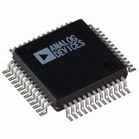
ADV7197KSZ Analog Devices Inc, ADV7197KSZ Datasheet

ADV7197KSZ
Specifications of ADV7197KSZ
Related parts for ADV7197KSZ
ADV7197KSZ Summary of contents
Page 1
GENERAL DESCRIPTION The ADV7197 is a triple, high-speed, digital-to-analog encoder on a single monolithic chip. It consists of three high-speed video D/A converters with TTL-compatible inputs. The ADV7197 has three separate 10-bit-wide input ports that accept data in 4:4:4 ...
Page 2
ADV7197–SPECIFICATIONS ( SPECIFICATIONS 70 C] unless otherwise noted.) Parameter STATIC PERFORMANCE Resolution Integral Nonlinearity Differential Nonlinearity DIGITAL OUTPUTS Output High Voltage Output Low Voltage Three-State ...
Page 3
AA 3.3 V SPECIFICATIONS unless otherwise noted.) Parameter STATIC PERFORMANCE Resolution Integral Nonlinearity Differential Nonlinearity DIGITAL OUTPUTS Output High Voltage Output Low Voltage Three-State Leakage Current Three-State Output Capacitance DIGITAL AND ...
Page 4
ADV7197–SPECIFICATIONS 5 V DYNAMIC–SPECIFICATIONS Parameter Luma Bandwidth Chroma Bandwidth Signal-to-Noise Ratio Chroma/Luma Delay Inequality Specifications subject to change without notice. 3.3 V DYNAMIC–SPECIFICATIONS Parameter Luma Bandwidth Chroma Bandwidth Signal-to-Noise Ratio Chroma/Luma Delay Inequality Specifications subject to change without notice. 5 ...
Page 5
V TIMING–SPECIFICATIONS P arameter 1 MPU PORT SCLOCK Frequency SCLOCK High Pulsewidth SCLOCK Low Pulsewidth Hold Time (Start Condition Setup Time (Start Condition Data Setup Time SDATA, SCLOCK Rise ...
Page 6
ADV7197 CLOCK PIXEL INPUT DATA t 11 CLOCK PIXEL INPUT DATA ... ... Cb0 Cb1 Cb2 Cb3 ... Cr0 Cr1 Cr2 Cr3 ... ...
Page 7
HSYNC VSYNC A DV PIXEL DATA CLK CYCLES FOR 1080i MIN CLK CYCLES FOR 720P MIN B = 236 CLK CYCLES FOR 1080i MIN B = 300 CLK CYCLES FOR 720P MIN t 3 ...
Page 8
ADV7197 1 ABSOLUTE MAXIMUM RATINGS V to GND . . . . . . . . . . . . . . . . . . . . . . . . . . . . . . . . ...
Page 9
Pin Mnemonic Input/Output 2–11 Y0–Y9 I 13, 52 GND G 14–23 Cr0–Cr9 I 24 CLKIN I 26, 33 AGND VSYNC TSYNC HSYNC/ 29 SYNC ...
Page 10
ADV7197 FUNCTIONAL DESCRIPTION Digital Inputs The digital inputs of the ADV7197 are TTL-compatible. 30-bit YCrCb or RGB pixel data in 4:4:4 format or 20-bit YCrCb pixel data in 4:2:2 format is latched into the device on the rising edge of ...
Page 11
A Logic “0” on the LSB of the first byte means that the master will write information to the peripheral. A Logic “1” on the LSB of the first byte means that the master will read information from the peripheral. ...
Page 12
ADV7197 MODE REGISTER 0 MR0 (MR07–MR00) (Address (SR4–SR0) = 00H) Figure 14 shows the various operations under the control of Mode Register 0. MR0 BIT DESCRIPTION Output Standard Selection (MR00–MR01) These bits are used to select the output levels from ...
Page 13
MR07 MR07 ZERO MUST BE WRITTEN TO THIS BIT DV POLARITY MR06 0 1 Table I must be followed when programming the control signals in Async Timing Mode. Table I. Truth Table SYNC TSYNC DV 1 –> ...
Page 14
ADV7197 MODE REGISTER 2 MR1 (MR27–MR20) (Address (SR4–SR0) = 02H) Figure 17 shows the various operations under the control of Mode Register 2. MR2 BIT DESCRIPTION Y Delay (MR20–MR22) With these bits it is possible to delay the Y signal ...
Page 15
MODE REGISTER 4 MR4 (MR47–MR40) (Address (SR4–SR0) = 04H) Figure 19 shows the various operations under the control of Mode Register 4. MR4 BIT DESCRIPTION Timing Reset (MR40) Toggling MR40 from low to high and low again resets the inter- ...
Page 16
ADV7197 COLOR Y CY (CY7–CY0) (Address (SR4–SR0) = 06H) CY7 CY6 CY5 CY4 CY3 CY7–CY0 COLOR Y VALUE Figure 21. Color Y Register COLOR CR CCR (CCR7–CCR0) (Address (SR4–SR0) = 07H) CCR7 CCR6 CCR5 CCR4 CCR3 CCR7–CCR0 COLOR CR VALUE ...
Page 17
Supply Decoupling Noise on the analog power plane can be further reduced by the use of decoupling capacitors. Optimum performance is achieved by the use of 0.1 µF ceramic capacitors. Each of group vidually ...
Page 18
ADV7197 Video Output Buffer and Optional Output Filter Output buffering is necessary in order to drive output devices, such as HDTV monitors. Analog Devices produces a range of suitable op amps for this application. A suitable op amp would be ...
Page 19
INPUT CODE EIA-770.3, STANDARD FOR Y 940 ACTIVE 64 EIA-770.3, STANDARD FOR Pr/Pb 960 ACTIVE 512 64 REGISTER SETTINGS Register Settings on Power-Up Address 00hex Mode Register 0 01hex Mode Register 1 02hex Mode Register 2 03hex Mode Register 3 ...
Page 20
ADV7197 747 748 749 750 FIELD 1 1124 1125 FIELD 2 561 562 VERTICAL BLANKING INTERVAL VERTICAL BLANKING INTERVAL VERTICAL BLANKING INTERVAL 563 564 565 566 ...


