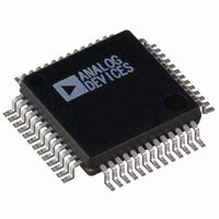
ADV7197KSZ Analog Devices Inc, ADV7197KSZ Datasheet - Page 13

ADV7197KSZ
Manufacturer Part Number
ADV7197KSZ
Description
IC DAC VID-HDTV 3CH-11BIT 52MQFP
Manufacturer
Analog Devices Inc
Type
Video Encoderr
Datasheet
1.ADV7197KS.pdf
(20 pages)
Specifications of ADV7197KSZ
Applications
HDTV
Voltage - Supply, Analog
3.15 V ~ 3.45 V
Mounting Type
Surface Mount
Package / Case
52-MQFP, 52-PQFP
Adc/dac Resolution
11b
Screening Level
Industrial
Package Type
MQFP
Pin Count
52
Lead Free Status / RoHS Status
Lead free / RoHS Compliant
Voltage - Supply, Digital
-
Lead Free Status / RoHS Status
Compliant, Lead free / RoHS Compliant
Table I must be followed when programming the control signals
in Async Timing Mode.
SYNC
1 –> 0
0
0 –> 1
1
1
MODE REGISTER 1
MR1 (MR17–MR10)
(Address (SR4–SR0) = 01H)
Figure 15 shows the various operations under the control of
Mode Register 1.
MR1 BIT DESCRIPTION
Pixel Data Enable (MR10)
When this bit is set to “0,” the pixel data input to the ADV7197
is blanked such that a black screen is output from the DACs.
TSYNC
0
0 –> 1
0 or 1
0 or 1
0 or 1
Table I. Truth Table
DV
0 or 1
0 or 1
0
0 –> 1
1 –> 0
TO THESE BITS
BE WRITTEN
MR17–MR15
ZERO MUST
BE WRITTEN
ZERO MUST
TO THIS BIT
MR17
MR07
MR07
50% Point of Falling Edge of
Tri-Level Horizontal Sync
Signal, a
25% Point of Rising Edge of
Tri-Level Horizontal Sync
Signal, b
50% Point of Falling Edge of
Tri-Level Horizontal Sync
Signal, c
50% Start of Active Video, d
50% End of Active Video, e
MR06
0
1
DV POLARITY
MR16
MR06
ACTIVE HIGH
ACTIVE LOW
MR05
0
1
INPUT STANDARD
MR15
MR05
1080I
720P
MR14
0
1
VBI OPEN
MR14
DISABLED
ENABLED
MR04
MR13
0
1
BE WRITTEN
ZERO MUST
TO THIS BIT
TEST PATTERN
HATCH/FRAME
MR04
HATCH
FIELD/FRAME
MR13
When this bit is set to “1,” pixel data is accepted at the input
pins and the ADV7197 outputs to the standard set in “Output
Standard Selection” (MR01–MR00). This bit also must be set
to “1” to enable output of the test pattern signals.
Input Format (MR11)
It is possible to input data in 4:2:2 format or in 4:4:4 format.
Test Pattern Enable (MR12)
Enables or disables the internal test pattern generator.
Test Pattern Hatch/Frame (MR13)
If this bit is set to “0,” a cross hatch test pattern is output from
the ADV7197. The cross hatch test pattern can be used to test
monitor convergence.
If this bit is set to “1,” a uniform colored frame/field test pattern
is output from the ADV7197.
The color of the lines or the frame/field is by default white but
can be programmed to be any color using the Color Y, Color
Cr, Color Cb Registers.
VBI Open (MR14)
This bit enables or disables the facility of VBI data insertion
during the Vertical Blanking Interval.
For this purpose Lines 7–20 in 1080i and Lines 6–25 in 720p
can be used for VBI data insertion.
Reserved (MR15–MR17)
A “0” must be written to these bits.
MR03
MR12
0
1
TEST PATTERN
MR03 MR02
0
0
1
1
ENABLE
MR12
INPUT CONTROL SIGNALS
MR01 MR00
0
0
1
1
DISABLED
ENABLED
OUTPUT STANDARD SELECTION
MR02
0
0
1
1
MR11
0
1
1
INPUT FORMAT
0
0
1
MR11
HSYNC\VSYNC/DV
EAV/SAV
TSYNC/SYNC/DV
RESERVED
4:4:4 YCrCb
4:2:2 YCrCb
MR01
EIA-770.3
RESERVED
FULL I/P RANGE
RESERVED
MR10
0
1
PIXEL DATA
ENABLE
MR10
DISABLED
ENABLED
MR00
ADV7197


