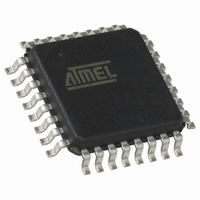
QT60248-ASG Atmel, QT60248-ASG Datasheet - Page 4

QT60248-ASG
Manufacturer Part Number
QT60248-ASG
Description
IC SENSOR QMATRIX 24CHAN 32TQFP
Manufacturer
Atmel
Series
QMatrix™, QProx™r
Type
Capacitiver
Datasheet
1.QT60168-ASG.pdf
(28 pages)
Specifications of QT60248-ASG
Number Of Inputs/keys
24 Key
Resolution (bits)
9, 11 b
Data Interface
Serial, SPI™
Voltage - Supply
3 V ~ 5 V
Current - Supply
25mA
Operating Temperature
-40°C ~ 105°C
Mounting Type
Surface Mount
Package / Case
32-TQFP, 32-VQFP
Output Type
Logic
Interface
SPI
Input Type
Logic
Operating Supply Voltage
3 V to 5 V
Maximum Operating Temperature
+ 105 C
Minimum Operating Temperature
- 40 C
Mounting Style
SMD/SMT
For Use With
427-1087 - BOARD EVAL QT60248-AS QMATRIX
Lead Free Status / RoHS Status
Lead free / RoHS Compliant
Other names
427-1108
Available stocks
Company
Part Number
Manufacturer
Quantity
Price
Company:
Part Number:
QT60248-ASG
Manufacturer:
ATMEL
Quantity:
101
Part Number:
QT60248-ASG
Manufacturer:
QUANTUM
Quantity:
20 000
For example:
The worst case response time is computed as:
For the above example values:
2.4 Oscillator
The oscillator is internal to the device. There is no facility for
external clocking.
2.5 Sample Capacitors; Saturation
The charge sampler capacitors on the Y pins should be the
values shown. They should be X7R or NP0 ceramics or PPS
film. The value of these capacitors is not critical but 4.7nF is
recommended for most cases.
Cs voltage saturation is shown in Figure 2-1. This nonlinearity
is caused by excessively negative voltage on Cs inducing
conduction in the pin protection diodes. This badly saturated
signal destroys key gain and introduces a strong thermal
coefficient which can cause 'phantom' detection. The cause of
this is usually from the burst length being too long, the Cs value
being too small, or the X-Y coupling being too large. Solutions
include loosening up the interdigitation of key structures,
separating X and Y lines on the PCB more, increasing Cs, and
decreasing the burst length.
Increasing Cs will make the part slower; decreasing burst
length will make it less sensitive. A better PCB layout and a
looser key structure (up to a point) have no negative effects.
Cs voltages should be observed on an oscilloscope with the
matrix layer bonded to the panel material; if the Rs side of any
Cs ramps more negative than -0.25 volts during any burst (not
counting overshoot spikes which are probe artifacts), there is a
potential saturation problem.
Figure 2-2 shows a defective waveform similar to that of 2-1,
but in this case the distortion is caused by excessive stray
capacitance coupling from the Y line to AC ground, for example
from running too near and too far alongside a ground trace,
ground plane, or other traces. The excess coupling causes the
charge-transfer effect to dissipate a significant portion of the
received charge from a key into the stray capacitance. This
phenomenon is more subtle; it can be best detected by
increasing BL to a high count and watching what the waveform
does as it descends towards and below -0.25V. The waveform
will appear deceptively straight, but it will slowly start to flatten
even before the -0.25V level is reached.
A correct waveform is shown in Figure 2-3. Note that the
bottom edge of the bottom trace is substantially straight
(ignoring the downward spikes).
Unlike other QT circuits, the Cs capacitor values on QT60xx8
devices have no effect on conversion gain. However they do
affect conversion time.
Unused Y lines should be left open.
lQ
NKE = Number of keys enabled = 20
FDIL = Fast detect integrator limit = 5
BS = Burst spacing = 0.5ms
FMEA = FMEA test time = 5ms
NDIL = Norm detect integrator Limit = 2
HPR = Host polling rate = 10ms
Tr = ((((20 + 5) * 0.5ms) + 5ms) * 2) + 10ms = 45ms
Tr = ((((NKE + FDIL) * BS) + FMEA) * NDIL) + HPR
4
2.6 Sample Resistors
There are 3 sample resistors (Rs) used to perform single-slope
ADC conversion of the acquired charge on each Cs capacitor.
These resistors directly control acquisition gain: larger values of
Rs will proportionately increase signal gain. Values of Rs can
range from 380K ohms to 1M ohms. 470K ohms is a
reasonable value for most purposes.
Unused Y lines do not require an Rs resistor.
2.7 Signal Levels
Quantum’s QmBtn™ software makes it is easy to observe the
absolute level of signal received by the sensor on each key.
The signal values should normally be in the range from 250 to
750 counts with properly designed key shapes and values of
Rs. However, long adjacent runs of X and Y lines can also
artificially boost the signal values, and induce signal saturation:
this is to be avoided. The X-to-Y coupling should come mostly
from intra-key electrode coupling, not from stray X-to-Y trace
coupling.
QmBtn software is available free of charge on Quantum’s
website.
The signal swing from the smallest finger touch should
preferably exceed 10 counts, with 15 being a reasonable target.
The signal threshold setting (NTHR) should be set to a value
guaranteed to be less than the signal swing caused by the
smallest touch.
(Burst too long, or Cs too small, or X-Y capacitance too large)
Figure 2-2 VCs - Poor Gain, Non-Linear During Burst
Figure 2-1 VCs - Non-Linear During Burst
(Excess capacitance from Y line to Gnd)
Figure 2-3 Vcs - Correct
QT60248-AS R4.02/0405


