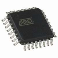
QT60248-ASG Atmel, QT60248-ASG Datasheet - Page 5

QT60248-ASG
Manufacturer Part Number
QT60248-ASG
Description
IC SENSOR QMATRIX 24CHAN 32TQFP
Manufacturer
Atmel
Series
QMatrix™, QProx™r
Type
Capacitiver
Datasheet
1.QT60168-ASG.pdf
(28 pages)
Specifications of QT60248-ASG
Number Of Inputs/keys
24 Key
Resolution (bits)
9, 11 b
Data Interface
Serial, SPI™
Voltage - Supply
3 V ~ 5 V
Current - Supply
25mA
Operating Temperature
-40°C ~ 105°C
Mounting Type
Surface Mount
Package / Case
32-TQFP, 32-VQFP
Output Type
Logic
Interface
SPI
Input Type
Logic
Operating Supply Voltage
3 V to 5 V
Maximum Operating Temperature
+ 105 C
Minimum Operating Temperature
- 40 C
Mounting Style
SMD/SMT
For Use With
427-1087 - BOARD EVAL QT60248-AS QMATRIX
Lead Free Status / RoHS Status
Lead free / RoHS Compliant
Other names
427-1108
Available stocks
Company
Part Number
Manufacturer
Quantity
Price
Company:
Part Number:
QT60248-ASG
Manufacturer:
ATMEL
Quantity:
101
Part Number:
QT60248-ASG
Manufacturer:
QUANTUM
Quantity:
20 000
Increasing the burst length (BL) parameter will increase the
signal strengths as will increasing the sampling resistor (Rs)
values.
2.8 Matrix Series Resistors
The X and Y matrix scan lines should use series resistors
(referred to as Rx and Ry respectively) for improved EMI
performance.
X drive lines require them in most cases to reduce edge rates
and thus reduce RF emissions. Typical values range from 1K to
20K ohms.
Y lines need them to reduce EMC susceptibility problems and in
some extreme cases, ESD. Typical Y values range around 1K
ohms. Y resistors act to reduce noise susceptibility problems by
forming a natural low-pass filter with the Cs capacitors.
It is essential that the Rx and Ry resistors and Cs capacitors be
placed very close to the chip. Placing these parts more than a
few millimeters away opens the circuit up for high frequency
interference problems (above 20MHz) as the trace lengths
between the components and the chip start to act as RF
antennae.
lQ
Figure 2-5 Probing X-Drive Waveforms With a Coin
Figure 2-4 X-Drive Pulse Roll-off and Dwell Time
Dwell time
Y gate
X drive
Lost charge due to
inadequate settling
before end of dwell time
5
The upper limits of Rx and Ry are reached when the signal
level and hence key sensitivity are clearly reduced. The limits of
Rx and Ry will depending on key geometry and stray
capacitance, and thus an oscilloscope is required to determine
optimum values of both.
The upper limit of Rx can vary depending on key geometry and
stray capacitance, and some experimentation and an
oscilloscope are required to determine optimum values.
Dwell time is the duration in which charge coupled from X to Y
is captured. Increasing Rx values will cause the leading edge of
the X pulses to increasingly roll off, causing the loss of captured
charge (and hence loss of signal strength) from the keys
(Figure 2-4). The dwell time of these parts is fixed at 375ns. If
the X pulses have not settled within 375ns, key gain will be
reduced; if this happens, either the stray capacitance on the X
line(s) should be reduced (by a layout change, for example by
reducing X line exposure to nearby ground planes or traces), or,
the Rx resistor needs to be reduced in value (or a combination
of both approaches).
One way to determine X line settling time is to monitor the fields
using a patch of metal foil or a small coin over the key (Figure
2-5). Only one key along a particular X line needs to be
observed, as each of the keys along that X line will be identical.
The 250ns dwell time should be exceed the observed 95%
settling of the X-pulse by 25% or more.
In almost all case, Ry should be set equal to Rx, which will
ensure that the charge on the Y line is fully captured into the Cs
capacitor.
2.9 Key Design
Circuits can be constructed out of a variety of materials
including flex circuits, FR4, and even inexpensive single-sided
CEM-1.
The actual internal pattern style is not as important as is the
need to achieve regular X and Y widths and spacings of
sufficient size to cover the desired graphical key area or a little
bit more; ~3mm oversize is acceptable in most cases, since the
key’s electric fields drop off near the edges anyway. The overall
key size can range from 10mm x 10mm up to 100mm x 100mm
but these are not hard limits. The keys can be any shape
including round, rectangular, square, etc. The internal pattern
‘T’ should ideally be similar to the complete thickness the fields need to
penetrate to the touch surface. Smaller dimensions will also work but will give
less signal strength. If in doubt, make the pattern coarser.
Figure 2-6 Recommended Key Structure
QT60248-AS R4.02/0405


