AD9847AKST Analog Devices Inc, AD9847AKST Datasheet - Page 9
AD9847AKST
Manufacturer Part Number
AD9847AKST
Description
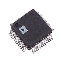
IC CCD SIGNAL PROC 10BIT 48-LQFP
Manufacturer
Analog Devices Inc
Type
CCD Signal Processor, 10-Bitr
Datasheet
1.AD9847AKSTZRL.pdf
(28 pages)
Specifications of AD9847AKST
Rohs Status
RoHS non-compliant
Input Type
Logic
Output Type
Logic
Interface
3-Wire Serial
Mounting Type
Surface Mount
Package / Case
48-LQFP
Analog Front End Type
CCD
Analog Front End Category
Video
Interface Type
Serial (3-Wire)
Sample Rate
40MSPS
Input Voltage Range
0.5V
Operating Supply Voltage (min)
2.7/3V
Operating Supply Voltage (typ)
3.3/5V
Operating Supply Voltage (max)
3.6/5.5V
Resolution
10b
Number Of Adc's
1
Power Supply Type
Analog/Digital
Operating Temp Range
-20C to 85C
Operating Temperature Classification
Commercial
Mounting
Surface Mount
Pin Count
48
Package Type
LQFP
Number Of Channels
1
Current - Supply
-
Lead Free Status / RoHS Status
Not Compliant
Available stocks
Company
Part Number
Manufacturer
Quantity
Price
Company:

Part Number:
AD9847AKST
Manufacturer:
AD
Quantity:
1 831
Company:
Part Number:
AD9847AKST
Manufacturer:
ADI
Quantity:
244
Part Number:
AD9847AKST
Manufacturer:
ADI/亚德诺
Quantity:
20 000
Company:
Part Number:
AD9847AKSTZ
Manufacturer:
Analog Devices Inc
Quantity:
10 000
Company:
Part Number:
AD9847AKSTZRL
Manufacturer:
Analog Devices Inc
Quantity:
10 000


REV. A
SERIAL INTERFACE TIMING
COMPLETE REGISTER LISTING
Register
oprmode
ctlmode
preventpdate
readback
vdhdpol
fieldval
hblkretime
tgcore_rstb
h12pol
h1posloc
h1negloc
NOTES
All addresses and default values are expressed in hexadecimal.
All registers are VD/HD updated as shown in Figure 3a, except for those that are SL updated.
SDATA
SCK
SL
SDATA
NOTES
1. MULTIPLE SEQUENTIAL REGISTERS MAY BE LOADED CONTINUOUSLY.
2. THE FIRST (LOWEST ADDRESS) REGISTER ADDRESS IS WRITTEN, FOLLOWED BY MULTIPLE 6-BIT DATA-WORDS.
3. THE ADDRESS WILL AUTOMATICALLY INCREMENT WITH EACH 6-BIT DATA-WORD (ALL SIX BITS MUST BE WRITTEN).
4. SL IS HELD LOW UNTIL THE LAST DESIRED REGISTER HAS BEEN LOADED.
5. NEW DATA IS UPDATED EITHER AT THE SL RISING EDGE OR AT THE HD FALLING EDGE AFTER THE NEXT VD FALLING EDGE.
SCK
AFE Operation Modes
AFE Control Modes
Prevents Loading of VD-Updated Registers
Enables Serial Register Readback Mode
VD/HD Active Polarity
Internal Field Pulse Value
Retimes the H1 hblk to Internal Clock
Reset Bar Signal for Internal TG Core
H1/H2 Polarity Control
H1 Positive Edge Location
H1 Negative Edge Location
SL
VD
Description
HD
A0
NOTES
1. SDATA BITS ARE LATCHED ON SCK RISING EDGES.
2. 14 SCK EDGES ARE NEEDED TO WRITE ADDRESS AND DATA BITS.
3. FOR 16-BIT SYSTEMS, TWO EXTRA DUMMY BITS MAY BE WRITTEN. DUMMY BITS ARE IGNORED.
4. NEW DATA IS UPDATED EITHER AT THE SL RISING EDGE OR AT THE HD FALLING EDGE AFTER THE NEXT VD FALLING EDGE.
5. VD/HD UPDATE POSITION MAY BE DELAYED TO ANY HD FALLING EDGE IN THE FIELD USING THE UPDATE REGISTER.
A1
A0
t
A2
DS
t
A1
LS
A3
A2
A4
A3
A5
Figure 3b. Continuous Serial Write Operation
t
A4
DH
A6
A5
Figure 3a. Serial Write Operation
A7
Table I. SL Updated Registers
A6
D0
A7
DATA FOR STARTING
REGISTER ADDRESS
D1
D0
D2
D1
–9–
D3
Register
h1drv
h2drv
h3drv
h4drv
rgpol
rgposloc
rgnegloc
rgdrv
shpposloc
shdposloc
D2
D4
D3
D5
t
D4
LH
D0
D5
D1
REGISTER ADDRESS
SL UPDATED
XX
H1 Drive Current
H2 Drive Current
H3 Drive Current
H4 Drive Current
RG Polarity
RG Positive Edge Location
RG Negative Edge Location
RG Drive Current
SHP Sample Location
SHD Sample Location
Description
DATA FOR NEXT
D2
XX
D3
D4
D5
VD/HD UPDATED
D0
D1
D2
AD9847
...
...
...
Related parts for AD9847AKST
Image
Part Number
Description
Manufacturer
Datasheet
Request
R

Part Number:
Description:
±1.7g Dual-Axis IMEMS Accelerometer Evaluation Board
Manufacturer:
Analog Devices Inc
Datasheet:

Part Number:
Description:
Inertial Sensor Evaluation System
Manufacturer:
Analog Devices Inc
Datasheet:
Part Number:
Description:
Manufacturer:
Analog Devices Inc
Datasheet:
Part Number:
Description:
Manufacturer:
Analog Devices Inc
Datasheet:
Part Number:
Description:
Manufacturer:
Analog Devices Inc
Datasheet:
Part Number:
Description:
Manufacturer:
Analog Devices Inc
Datasheet:
Part Number:
Description:
Manufacturer:
Analog Devices Inc
Datasheet:
Part Number:
Description:
Manufacturer:
Analog Devices Inc
Datasheet:
Part Number:
Description:
Manufacturer:
Analog Devices Inc
Datasheet:
Part Number:
Description:
Manufacturer:
Analog Devices Inc
Datasheet:
Part Number:
Description:
Manufacturer:
Analog Devices Inc
Datasheet:
Part Number:
Description:
Manufacturer:
Analog Devices Inc
Datasheet:
Part Number:
Description:
Manufacturer:
Analog Devices Inc
Datasheet: