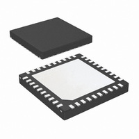
DS25BR204TSQ/NOPB National Semiconductor, DS25BR204TSQ/NOPB Datasheet - Page 7

DS25BR204TSQ/NOPB
Manufacturer Part Number
DS25BR204TSQ/NOPB
Description
IC REPEATER 3.125GBPS 1:4 40LLP
Manufacturer
National Semiconductor
Type
Repeaterr
Datasheet
1.DS25BR204TSQNOPB.pdf
(16 pages)
Specifications of DS25BR204TSQ/NOPB
Tx/rx Type
LVDS
Delay Time
600ps
Capacitance - Input
1.7pF
Voltage - Supply
3 V ~ 3.6 V
Current - Supply
185mA
Mounting Type
Surface Mount
Package / Case
40-LLP
Lead Free Status / RoHS Status
Lead free / RoHS Compliant
Other names
DS25BR204TSQTR
Available stocks
Company
Part Number
Manufacturer
Quantity
Price
Company:
Part Number:
DS25BR204TSQ/NOPB
Manufacturer:
NSC
Quantity:
500
JITTER PERFORMANCE WITH EQ = On, PE = On (Note 11)(Figure 8 Figure 9
t
t
t
t
t
t
RJ1BD
RJ2BD
DJ1BD
DJ2BD
TJ1BD
TJ2BD
Note 9: The Electrical Characteristics tables list guaranteed specifications under the listed Recommended Operating Conditions except as otherwise modified
or specified by the Electrical Characteristics Conditions and/or Notes. Typical specifications are estimations only and are not guaranteed.
Note 10: Typical values represent most likely parametric norms for V
product characterization and are not guaranteed.
Note 11: Specification is guaranteed by characterization and is not tested in production.
Note 12: t
going edge of the same channel.
Note 13: t
all outputs).
Note 14: t
devices at the same V
Note 15: Measured on a clock edge with a histogram and an acummulation of 1500 histogram hits. Input stimulus jitter is subtracted geometrically.
Note 16: Tested with a combination of the 1100000101 (K28.5+ character) and 0011111010 (K28.5- character) patterns. Input stimulus jitter is subtracted
algebraically.
Note 17: Measured on an eye diagram with a histogram and an acummulation of 3500 histogram hits. Input stimulus jitter is subtracted.
Symbol
SKD1
SKD2
SKD3
, |t
, Channel to Channel Skew, is the difference in propagation delay (t
, Part to Part Skew, is defined as the difference between the minimum and maximum differential propagation delays. This specification applies to
PLHD
Random Jitter (RMS Value)
Input Test Channel D
Output Test Channel B
(Note 15)
Deterministic Jitter (Peak to Peak)
Input Test Channel D
Output Test Channel B
(Note 16)
Total Jitter (Peak to Peak)
Input Test Channel D
Output Test Channel B
(Note 17)
− t
CC
PHLD
and within 5°C of each other within the operating temperature range.
|, Pulse Skew, is the magnitude difference in differential propagation delay time between the positive going edge and the negative
Parameter
CC
V
V
Clock (RZ)
V
V
K28.5 (NRZ)
V
V
PRBS-23 (NRZ)
= +3.3V and T
ID
CM
ID
CM
ID
CM
= 350 mV
= 350 mV
= 350 mV
= 1.2V
= 1.2V
= 1.2V
7
PLHD
A
or t
= +25°C, and at the Recommended Operation Conditions at the time of
Conditions
PHLD
) among all output channels in Broadcast mode (any one input to
2.5 Gbps
3.125 Gbps
2.5 Gbps
3.125 Gbps
2.5 Gbps
3.125 Gbps
Min
0.07
0.08
Typ
0.5
0.5
10
8
Max
0.12
0.15
www.national.com
20
21
1
1
Units
UI
UI
ps
ps
ps
ps
P-P
P-P


