LMH0344SQE/NOPB National Semiconductor, LMH0344SQE/NOPB Datasheet - Page 6
LMH0344SQE/NOPB
Manufacturer Part Number
LMH0344SQE/NOPB
Description
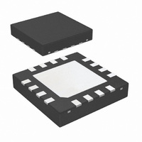
IC ADAPT CBL EQUALIZER 16-LLP
Manufacturer
National Semiconductor
Datasheet
1.LMH0344SQENOPB.pdf
(8 pages)
Specifications of LMH0344SQE/NOPB
Applications
Data Transport
Interface
Serial
Voltage - Supply
3.135 V ~ 3.465 V
Package / Case
16-LLP
Mounting Type
Surface Mount
Package
16LLP EP
Operating Temperature
-40 to 85 °C
Ic Function
Adaptive Cable Equalizer
Supply Voltage Range
3.135V To 3.465V
Operating Temperature Range
-40°C To +85°C
Digital Ic Case Style
LLP
No. Of Pins
16
Msl
MSL 1 - Unlimited
Rohs Compliant
Yes
Lead Free Status / RoHS Status
Lead free / RoHS Compliant
Other names
LMH0344SQE
LMH0344SQE
LMH0344SQETR
LMH0344SQE
LMH0344SQETR


www.national.com
Block Diagram
Device Operation
BLOCK DESCRIPTION
The Equalizer Filter block is a multi-stage adaptive filter. If
Bypass is high, the equalizer filter is disabled.
The DC Restoration / Level Control block receives the dif-
ferential signals from the equalizer filter block. This block
incorporates a self-biasing DC restoration circuit to fully DC
restore the signals. If Bypass is high, this function is disabled.
The signals before and after the DC Restoration / Level Con-
trol block are used to generate the Automatic Equalization
Control (AEC) signal. This control signal sets the gain and
bandwidth of the equalizer filter. The loop response in the
AEC block is controlled by an external 1µF capacitor placed
across the AEC+ and AEC- pins.
The Carrier Detect / Mute block generates the carrier detect
signal and controls the mute function of the output. This block
utilizes the CD and MUTE signals along with Mute Reference
(MUTE
The Output Driver produces SDO and SDO.
MUTE REFERENCE (MUTE
The mute reference sets the threshold for CD and (with CD
tied to MUTE) determines the amount of cable to equalize
before automatically muting the outputs. This is set by apply-
ing a voltage inversely proportional to the length of cable to
equalize. The applied voltage must be greater than the
MUTE
the CD threshold. As the applied MUTE
creased, the amount of cable that can be equalized before
REF
REF
floating voltage (typically 1.3V) in order to change
).
REF
)
REF
voltage is in-
6
carrier detect is de-asserted and the outputs are muted is de-
creased. MUTE
ground for maximum equalization before muting.
CARRIER DETECT (CD) AND MUTE
Carrier detect CD indicates if a valid signal is present at the
LMH0344 input. If MUTE
old will be altered accordingly. CD provides a high voltage
when no signal is present at the LMH0344 input. CD is low
when a valid input signal is detected.
MUTE can be used to manually mute or enable SDO and
SDO. Applying a high input to MUTE will mute the LMH0344
outputs by forcing the output to a logic zero. Applying a low
input will force the outputs to be active.
CD and MUTE may be tied together to automatically mute the
output when no input signal is present.
INPUT INTERFACING
The LMH0344 accepts either differential or single-ended in-
put. The input must be AC coupled. Transformer coupling is
not supported.
The LMH0344 correctly handles equalizer pathological sig-
nals for standard definition and high definition serial digital
video, as described in SMPTE RP 178 and RP 198, respec-
tively.
OUTPUT INTERFACING
The SDO and SDO outputs are internally loaded with 50Ω.
They produce a 750 mV
375 mV
P-P
single-ended output.
REF
may be left unconnected or connected to
REF
is used, the carrier detect thresh-
P-P
differential output, or a
20199002
Related parts for LMH0344SQE/NOPB
Image
Part Number
Description
Manufacturer
Datasheet
Request
R

Part Number:
Description:
IC ADAPT CBL EQUALIZER 16-LLP
Manufacturer:
National Semiconductor
Datasheet:

Part Number:
Description:
3gbps Hd/sd Sdi Adaptive Cable Equalizer
Manufacturer:
National Semiconductor Corporation

Part Number:
Description:
National Semiconductor [8-Bit D/A Converter]
Manufacturer:
National Semiconductor
Datasheet:
Part Number:
Description:
National Semiconductor [Media Coprocessor]
Manufacturer:
National Semiconductor
Datasheet:
Part Number:
Description:
Digitally Controlled Tone and Volume Circuit with Stereo Audio Power Amplifier, Microphone Preamp Stage and National 3D Sound
Manufacturer:
National Semiconductor
Datasheet:
Part Number:
Description:
Digitally Controlled Tone and Volume Circuit with Stereo Audio Power Amplifier, Microphone Preamp Stage and National 3D Sound
Manufacturer:
National Semiconductor
Datasheet:
Part Number:
Description:
AC97 Rev 2 Codec with Sample Rate Conversion and National 3D Sound
Manufacturer:
National Semiconductor
Part Number:
Description:
Manufacturer:
National Semiconductor
Datasheet:
Part Number:
Description:
Manufacturer:
National Semiconductor
Datasheet:
Part Number:
Description:
General Purpose, Low Voltage, Low Power, Rail-to-Rail Output Operational Amplifiers
Manufacturer:
National Semiconductor
Datasheet:
Part Number:
Description:
8-bit 20 MSPS flash A/D converter.
Manufacturer:
National Semiconductor
Datasheet:
Part Number:
Description:
Low Noise Quad Operational Amplifier
Manufacturer:
National Semiconductor
Datasheet:
Part Number:
Description:
Quad Differential Line Receivers
Manufacturer:
National Semiconductor
Datasheet:
Part Number:
Description:
Quad High Speed Trapezoidal? Bus Transceiver
Manufacturer:
National Semiconductor
Datasheet: