AD9887AKS-100 Analog Devices Inc, AD9887AKS-100 Datasheet - Page 10
AD9887AKS-100
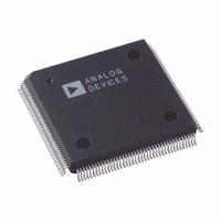
Manufacturer Part Number
AD9887AKS-100
Description
IC INTRFACE ANALOG/DVI 160-MQFP
Manufacturer
Analog Devices Inc
Datasheet
1.AD9887AKSZ-100.pdf
(40 pages)
Specifications of AD9887AKS-100
Rohs Status
RoHS non-compliant
Applications
Graphic Cards, VGA Interfaces
Interface
Analog and Digital
Voltage - Supply
3.15 V ~ 3.45 V
Package / Case
160-MQFP, 160-PQFP
Mounting Type
Surface Mount


AD9887
CLAMP
COAST
CKEXT
CKINV
External Clamp Input (Optional)
This logic input may be used to define the
time during which the input signal is clamped
to the reference dc level, (ground for RGB or
midscale for YUV). It should be exercised
when the reference dc level is known to be
present on the analog input channels, typically
during the back porch of the graphics signal.
The CLAMP pin is enabled by setting control
bit EXTCLMP to 1, (the default power-up is 0).
When disabled, this pin is ignored and the
clamp timing is determined internally by
counting a delay and duration from the trailing
edge of the HSYNC input. The logic sense of
this pin is controlled by CLAMPOL. When
not used, this pin must be grounded and
EXTCLMP programmed to 0.
Clock Generator Coast Input (Optional)
This input may be used to cause the pixel clock
generator to stop synchronizing with HSYNC
and continue producing a clock at its current
frequency and phase. This is useful when
processing signals from sources that fail to
produce horizontal sync pulses when in the
vertical interval. The COAST signal is generally
not required for PC-generated signals. Appli-
cations requiring COAST can do so through
the internal COAST found in the SYNC
processing engine.
The logic sense of this pin is controlled by
COAST Polarity.
When not used, this pin may be grounded and
COAST Polarity programmed to 1, or tied
HIGH and COAST Polarity programmed to 0.
COAST Polarity defaults to 1 at power-up.
External Clock Input (Optional)
This pin may be used to provide an external
clock to the AD9887, in place of the clock
internally generated from HSYNC.
It is enabled by programming EXTCLK to 1.
When an external clock is used, all other internal
functions operate normally. When unused, this
pin should be tied to V
EXTCLK programmed to 0. The clock phase
adjustment still operates when an external clock
source is used.
Sampling Clock Inversion (Optional)
This pin may be used to invert the pixel
sampling clock, which has the effect of
shifting the sampling phase 180°. This is in
support of Alternate Pixel Sampling mode,
wherein higher-frequency input signals (up
to 280 Mpps) may be captured by first sam-
pling the odd pixels, then capturing the even
pixels on the subsequent frame.
DD
or to GROUND, and
Outputs
D
D
D
D
D
D
DATACK
DATACK
R
R
G
G
B
B
A
B
A
B
A
B
7-0
7-0
7-0
7-0
7-0
7-0
This pin should be exercised only during blanking
intervals (typically vertical blanking) as it may
produce several samples of corrupted data during
the phase shift.
CKINV should be grounded when not used.
Data Output, Red Channel, Port A
Data Output, Red Channel, Port B
Data Output, Green Channel, Port A
Data Output, Green Channel, Port B
Data Output, Blue Channel, Port A
Data Output, Blue Channel, Port B
These are the main data outputs. Bit 7 is the MSB.
Each channel has two ports. When the part is
operated in single-channel mode (DEMUX = 0),
all data are presented to Port A, and Port B is
placed in a high-impedance state.
Programming DEMUX to 1 established dual-
channel mode, wherein alternate pixels are
presented to Port A and Port B of each chan-
nel. These will appear simultaneously, two
pixels presented at the time of every second
input pixel, when PAR is set to 1 (parallel
mode). When PAR = 0, pixel data appear
alternately on the two ports, one new sample
with each incoming pixel (interleaved mode).
In dual channel mode, the first pixel after
HSYNC is routed to Port A. The second pixel
goes to Port B, the third to A, etc.
The delay from pixel sampling time to output is
fixed. When the sampling time is changed by
adjusting the PHASE register, the output timing is
shifted as well. The DATACK, DATACK, and
HSOUT outputs are also moved, so the timing
relationship among the signals is maintained.
Data Output Clock
Data Output Clock Complement
Differential data clock output signals to be
used to strobe the output data and HSOUT
into external logic.
They are produced by the internal clock gen-
erator and are synchronous with the internal
pixel sampling clock.
When the AD9887 is operated in single-chan-
nel mode, the output frequency is equal to the
pixel sampling frequency. When operating in
dual channel mode, the clock frequency is one-
half the pixel frequency.
When the sampling time is changed by adjusting
the PHASE register, the output timing is shifted
as well. The Data, DATACK, DATACK, and
HSOUT outputs are all moved, so the timing
relationship among the signals is maintained.
Related parts for AD9887AKS-100
Image
Part Number
Description
Manufacturer
Datasheet
Request
R

Part Number:
Description:
BOARD EVAL FOR AD9887A
Manufacturer:
Analog Devices Inc
Datasheet:

Part Number:
Description:
±1.7g Dual-Axis IMEMS Accelerometer Evaluation Board
Manufacturer:
Analog Devices Inc
Datasheet:
Part Number:
Description:
Inertial Sensor Evaluation System
Manufacturer:
Analog Devices Inc
Datasheet:
Part Number:
Description:
Manufacturer:
Analog Devices Inc
Datasheet:
Part Number:
Description:
Manufacturer:
Analog Devices Inc
Datasheet:
Part Number:
Description:
Manufacturer:
Analog Devices Inc
Datasheet:
Part Number:
Description:
Manufacturer:
Analog Devices Inc
Datasheet:
Part Number:
Description:
Manufacturer:
Analog Devices Inc
Datasheet:
Part Number:
Description:
Manufacturer:
Analog Devices Inc
Datasheet:
Part Number:
Description:
Manufacturer:
Analog Devices Inc
Datasheet:
Part Number:
Description:
Manufacturer:
Analog Devices Inc
Datasheet:
Part Number:
Description:
Manufacturer:
Analog Devices Inc
Datasheet:
Part Number:
Description:
Manufacturer:
Analog Devices Inc
Datasheet: