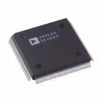
AD9887AKS-100 Analog Devices Inc, AD9887AKS-100 Datasheet - Page 30

AD9887AKS-100
Manufacturer Part Number
AD9887AKS-100
Description
IC INTRFACE ANALOG/DVI 160-MQFP
Manufacturer
Analog Devices Inc
Datasheet
1.AD9887AKSZ-100.pdf
(40 pages)
Specifications of AD9887AKS-100
Rohs Status
RoHS non-compliant
Applications
Graphic Cards, VGA Interfaces
Interface
Analog and Digital
Voltage - Supply
3.15 V ~ 3.45 V
Package / Case
160-MQFP, 160-PQFP
Mounting Type
Surface Mount
AD9887
06
Hsync Pulsewidth
07
INPUT GAIN
08
09
0A
INPUT OFFSET
0B
7–0 Hsync Output Pulsewidth
7–0 Red Channel Gain Adjust
7–0 Clamp Duration
An 8-bit register that sets the duration of the internally
generated clamp.
When EXTCLMP = 0, a clamp signal is generated inter-
nally, at a position established by the clamp placement
and for a duration set by the clamp duration. Clamping is
started (clamp placement) pixel periods after the trailing
edge of Hsync, and continues for (clamp duration) pixel
periods. The clamp duration may be programmed to any
value between 1 and 255. A value of 0 is not supported.
For the best results, the clamp duration should be set to
include the majority of the black reference signal time that
follows the Hsync signal trailing edge. Insufficient clamp-
ing time can produce brightness changes at the top of the
screen, and a slow recovery from large changes in the
Average Picture Level (APL), or brightness.
When EXTCLMP = 1, this register is ignored.
An 8-bit register that sets the duration of the Hsync
output pulse.
The leading edge of the Hsync output is triggered by the
internally generated, phase-adjusted PLL feedback clock.
The AD9887 then counts a number of pixel clocks equal
to the value in this register. This triggers the trailing edge
of the Hsync output, which is also phase-adjusted.
An 8-bit word that sets the gain of the RED channel.
The AD9887 can accommodate input signals with a
full-scale range of between 0.5 V and 1.5 V p-p. Setting
REDGAIN to 255 corresponds to an input range of 1.0 V.
A REDGAIN of 0 establishes an input range of 0.5 V.
Note that INCREASING REDGAIN results in the picture
having LESS CONTRAST (the input signal uses fewer
of the available converter codes). See Figure 3.
7–0 Green Channel Gain Adjust
An 8-bit word that sets the gain of the GREEN channel.
See REDGAIN (08).
7–0 Blue Channel Gain Adjust
An 8-bit word that sets the gain of the BLUE channel.
See REDGAIN (08).
7–1 Red Channel Offset Adjust
A 7-bit offset binary word that sets the dc offset of the RED
channel. One LSB of offset adjustment equals approximately
one LSB change in the ADC offset. Therefore, the absolute
magnitude of the offset adjustment scales as the gain of the
channel is changed. A nominal setting of 63 results in the
channel nominally clamping the back porch (during the
clamping interval) to Code 00. An offset setting of 127
results in the channel clamping to Code 63 of the ADC. An
offset setting of 0 clamps to code –63 (off the bottom of
the range). Increasing the value of Red Offset DECREASES
the brightness of the channel.
0C
0D
MODE CONTROL 1
0E
0E
0E
7–1 Green Channel Offset Adjust
A 7-bit offset binary word that sets the dc offset of the
GREEN channel. See REDOFST (0B).
7–1 Blue Channel Offset Adjust
A 7-bit offset binary word that sets the dc offset of the
GREEN channel. See REDOFST (0B).
7 Channel Mode
A bit that determines whether all pixels are presented to a
single port (A), or alternating pixels are demultiplexed to
Ports A and B.
DEMUX
0
1
When DEMUX = 0, Port B outputs are in a high-impedance
state. The maximum data rate for single port mode is
100 MHz. The timing diagrams show the effects of this option.
The power-up default value is 1.
6 Output Mode
A bit that determines whether all pixels are presented to
Port A and Port B simultaneously on every second
DATACK rising edge, or alternately on port A and Port B
on successive DATACK rising edges.
PARALLEL
0
1
When in single port mode (DEMUX = 0), this bit is ig-
nored. The timing diagrams show the effects of this option.
The power-up default value is PARALLEL = 1.
5 Output Port Phase
One bit that determines whether even pixels or odd pixels
go to Port A.
OUTPHASE
0
1
In normal operation (OUTPHASE = 1), when operating
in dual-port output mode (DEMUX = 1), the first sample
after the Hsync leading edge is presented at Port A. Every
subsequent ODD sample appears at Port A. All EVEN
samples go to Port B.
When OUTPHASE = 0, these ports are reversed and the
first sample goes to Port B.
Table XIV. Output Port Phase Settings
Table XII. Channel Mode Settings
Table XIII. Output Mode Settings
Function
All Data Goes to Port A
Alternate Pixels Go to Port A and Port B
Function
Data Is Interleaved
Data Is Simultaneous On Every Other
Data Clock
First Pixel After Hsync
Port B
Port A


