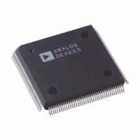
AD9887AKS-100 Analog Devices Inc, AD9887AKS-100 Datasheet - Page 15

AD9887AKS-100
Manufacturer Part Number
AD9887AKS-100
Description
IC INTRFACE ANALOG/DVI 160-MQFP
Manufacturer
Analog Devices Inc
Datasheet
1.AD9887AKSZ-100.pdf
(40 pages)
Specifications of AD9887AKS-100
Rohs Status
RoHS non-compliant
Applications
Graphic Cards, VGA Interfaces
Interface
Analog and Digital
Voltage - Supply
3.15 V ~ 3.45 V
Package / Case
160-MQFP, 160-PQFP
Mounting Type
Surface Mount
Sync-on-Green
The Sync-on-Green input operates in two steps. First, it sets a
baseline clamp level from the incoming video signal with a
negative peak detector. Second, it sets the Sync trigger level
(nominally 150 mV above the negative peak). The exact trigger
level is variable and can be programmed via register 11H. The
Sync-on-Green input must be ac-coupled to the green analog
input through its own capacitor as shown in Figure 4. The value
of the capacitor must be 1 nF ± 20%. If Sync-on-Green is not
used, this connection is not required and SOGIN should be left
unconnected. (Note: The Sync-on-Green signal is always nega-
tive polarity.) Please refer to the Sync Processing section for more
information.
Clock Generation
A Phase Locked Loop (PLL) is employed to generate the pixel
clock. The HSYNC input provides a reference frequency for the
PLL. A Voltage Controlled Oscillator (VCO) generates a much
higher pixel clock frequency. This pixel clock is divided by the
PLL divide value (Registers 01H and 02H) and phase compared
with the Hsync input. Any error is used to shift the VCO fre-
quency and maintain lock between the two signals.
The stability of this clock is a very important element in provid-
ing the clearest and most stable image. During each pixel time,
there is a period when the signal is slewing from the old pixel
amplitude and settling at its new value. Then there is a time
when the input voltage is stable, before the signal must slew to a
new value (see Figure 5). The ratio of the slewing time to the
stable time is a function of the bandwidth of the graphics DAC
and the bandwidth of the transmission system (cable and termi-
nation). It is also a function of the overall pixel rate. Clearly, if the
dynamic characteristics of the system remain fixed, the slewing
and settling times are likewise fixed. This time must be sub-
tracted from the total pixel period, leaving the stable period. At
higher pixel frequencies, the total cycle time is shorter, and the
stable pixel time becomes shorter as well.
14
12
10
8
6
4
2
0
47nF
47nF
47nF
1nF
PIXEL CLOCK – MHz
R
B
G
SOGIN
AIN
AIN
AIN
Any jitter in the clock reduces the precision with which the
sampling time can be determined, and must also be subtracted
from the stable pixel time.
Considerable care has been taken in the design of the AD9887’s
clock generation circuit to minimize jitter. As indicated in Fig-
ure 6, the clock jitter of the AD9887 is less than 6% of the total
pixel time in all operating modes, making the reduction in the
valid sampling time due to jitter negligible.
The PLL characteristics are determined by the loop filter
design, by the PLL charge pump current and by the VCO range
setting. The loop filter design is illustrated in Figure 7. Recom-
mended settings of VCO range and charge pump current for
VESA standard display modes are listed in Table VII.
Four programmable registers are provided to optimize the per-
formance of the PLL. These registers are:
1. The 12-Bit Divisor Register. The input Hsync frequencies
2. The 2-Bit VCO Range Register. To lower the sensitivity of
range from 15 kHz to 110 kHz. The PLL multiplies the
frequency of the Hsync signal, producing pixel clock fre-
quencies in the range of 12 MHz to 140 MHz. The Divisor
Register controls the exact multiplication factor. This register
may be set to any value between 221 and 4095. (The divide
ratio that is actually used is the programmed divide ratio
plus one.)
the output frequency to noise on the control signal, the VCO
operating frequency range is divided into four overlapping
regions. The VCO Range register sets this operating range.
Because there are only four possible regions, only the two
least-significant bits of the VCO Range register are used.
The frequency ranges for the lowest and highest regions
are shown in Table V.
PIXEL CLOCK
C
P
0.0039 F
INVALID SAMPLE TIMES
FILT
R
C
Z
Z
3.3k
0.039 F
PV
AD9887
D


