DS90CP22M-8/NOPB National Semiconductor, DS90CP22M-8/NOPB Datasheet - Page 2
DS90CP22M-8/NOPB
Manufacturer Part Number
DS90CP22M-8/NOPB
Description
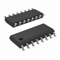
IC CROSSPOINT SWITCH 2X2 16SOIC
Manufacturer
National Semiconductor
Datasheet
1.DS90CP22M-8NOPB.pdf
(10 pages)
Specifications of DS90CP22M-8/NOPB
Function
Crosspoint Switch
Circuit
1 x 2:2
Voltage Supply Source
Single Supply
Voltage - Supply, Single/dual (±)
3 V ~ 3.6 V
Current - Supply
98mA
Operating Temperature
-40°C ~ 85°C
Mounting Type
Surface Mount
Package / Case
16-SOIC (0.154", 3.90mm Width)
For Use With
LVDSCP22EVK - EVALUATION BOARD FOR DS90CP22
Lead Free Status / RoHS Status
Lead free / RoHS Compliant
Other names
*DS90CP22M-8
*DS90CP22M-8/NOPB
DS90CP22M-8
*DS90CP22M-8/NOPB
DS90CP22M-8
Available stocks
Company
Part Number
Manufacturer
Quantity
Price
Company:

Part Number:
DS90CP22M-8/NOPB
Manufacturer:
NS
Quantity:
90


www.national.com
CMOS/TTL DC SPECIFICATIONS (EN0,EN1,SEL0,SEL1)
V
V
I
I
V
LVDS OUTPUT DC SPECIFICATIONS (OUT0,OUT1)
V
ΔV
V
ΔV
I
I
I
I
LVDS RECEIVER DC SPECIFICATIONS (IN0,IN1)
V
V
V
I
SUPPLY CURRENT
I
I
IH
IL
OZ
OFF
OS
OSB
IN
CCD
CCZ
Supply Voltage (V
CMOS/TTL Input Voltage (EN0,
EN1, SEL0, SEL1)
LVDS Receiver Input Voltage (IN
+, IN−)
LVDS Driver Output Voltage (OUT
+, OUT−)
LVDS Output Short Circuit Current
Junction Temperature
Storage Temperature Range
Lead Temperature
Maximum Package Power Dissipation at 25°C
Symbol
IH
IL
CL
OD
OS
TH
TL
CMR
Absolute Maximum Ratings
If Military/Aerospace specified devices are required,
please contact the National Semiconductor Sales Office/
Distributors for availability and specifications.
Electrical Characteristics
Over recommended operating supply and temperature ranges unless otherwise specified
Note 1: “Absolute Maximum Ratings” are these beyond which the safety of the device cannot be guaranteed. They are not meant to imply that the device should
be operated at these limits. The table of “Electrical Characteristics” provides conditions for actual device operation.
Note 2: All typical are given for V
Note 3: V
OD
OS
(Soldering, 4 sec.)
OS
High Level Input Voltage
Low Level Input Voltage
High Level Input Current
Low Level Input Current
Input Clamp Voltage
Differential Output Voltage
Change in V
Offset Voltage (Note 3)
Change in V
Output TRI-STATE
Power-Off Leakage Current
Output Short Circuit Current
Both Outputs Short Circuit Current
Differential Input High Threshold
Differential Input Low Threshold
Common Mode Voltage Range
Input Current
Total Supply Current
TRI-STATE Supply Current
is defined and measured on the ATE as (V
CC
)
OD
OS
Parameter
between Complimentary Output States
between Complimentary Output States
CC
®
= +3.3V and T
Current
−0.3V to (V
A
= +25°C, unless otherwise stated.
−65°C to +150°C
OH
+ V
(Note 1)
−0.3V to +4V
−0.3V to +4V
−0.3V to +4V
OL
Continuous
CC
) / 2.
V
V
I
R
R
TRI-STATE Output,
V
V
V
V
V
Vcc = 3.3V
V
V
V
R
EN0 = EN1 = High
EN0 = EN1 = Low
CL
+150°C
+260°C
+ 0.3V)
IN
IN
OUT
CC
OUT+
OUT+
CM
ID
IN
IN
L
L
L
= 75Ω
= 75Ω, V
= 75Ω, C
= −18 mA
= 3.6V or 2.0V; V
= 0V or 0.8V; V
= 100mV, Vcc = 3.3V
= +3.0V, V
= 0V, V
= 0V; V
= +0.05V or +1.2V or +3.25V,
= V
OR V
AND V
CC
2
CC
or GND
OUT
OUT−
CC
L
OUT−
= 5 pF,
ESD Rating:
Supply Voltage (V
Receiver Input Voltage
Operating Free Air Temperature
= 3.6V or 0V
CC
Conditions
= 3.3V, T
Recommended Operating
Conditions
= 3.6V or GND
16L SOIC
16L SOIC Package Derating
16L TSSOP
16L TSSOP Package Derating
(HBM, 1.5kΩ, 100pF)
(EIAJ, 0Ω, 200pF)
= 0V
= 3.6V or 0V
= 0V
CC
CC
= 3.6V
= 3.6V
A
= 25°C
CC
)
−100
GND
0.05
Min
270
285
2.0
1.0
11.48 mW/°C above +25°C
9.6 mW/°C above +25°C
−0.8
Typ
−15
−30
365
365
1.2
Min Typ Max Unit
+7
±1
±1
±1
±1
±1
98
43
3.0
-40 +25 +85
0
0
0
3.3
+100
Max
−1.5
1.45
3.25
V
+20
±10
475
440
±10
±10
−25
−50
±10
±10
125
0.8
35
35
55
CC
V
3.6
CC
1.435 W
0.866 W
> 250 V
> 5 kV
Units
mV
mV
mV
mV
mA
mA
mV
mV
mA
mA
μA
μA
μA
μA
μA
μA
°C
V
V
V
V
V
V
V
s
Related parts for DS90CP22M-8/NOPB
Image
Part Number
Description
Manufacturer
Datasheet
Request
R

Part Number:
Description:
Line Receiver IC
Manufacturer:
National Semiconductor
Datasheet:
Part Number:
Description:
National Semiconductor [8-Bit D/A Converter]
Manufacturer:
National Semiconductor
Datasheet:
Part Number:
Description:
National Semiconductor [Media Coprocessor]
Manufacturer:
National Semiconductor
Datasheet:
Part Number:
Description:
Digitally Controlled Tone and Volume Circuit with Stereo Audio Power Amplifier, Microphone Preamp Stage and National 3D Sound
Manufacturer:
National Semiconductor
Datasheet:
Part Number:
Description:
Digitally Controlled Tone and Volume Circuit with Stereo Audio Power Amplifier, Microphone Preamp Stage and National 3D Sound
Manufacturer:
National Semiconductor
Datasheet:
Part Number:
Description:
AC97 Rev 2 Codec with Sample Rate Conversion and National 3D Sound
Manufacturer:
National Semiconductor
Part Number:
Description:
Manufacturer:
National Semiconductor
Datasheet:
Part Number:
Description:
Manufacturer:
National Semiconductor
Datasheet:
Part Number:
Description:
General Purpose, Low Voltage, Low Power, Rail-to-Rail Output Operational Amplifiers
Manufacturer:
National Semiconductor
Datasheet:
Part Number:
Description:
8-bit 20 MSPS flash A/D converter.
Manufacturer:
National Semiconductor
Datasheet:
Part Number:
Description:
Low Noise Quad Operational Amplifier
Manufacturer:
National Semiconductor
Datasheet:
Part Number:
Description:
Quad Differential Line Receivers
Manufacturer:
National Semiconductor
Datasheet:
Part Number:
Description:
Quad High Speed Trapezoidal? Bus Transceiver
Manufacturer:
National Semiconductor
Datasheet:
Part Number:
Description:
Dual Line Receiver
Manufacturer:
National Semiconductor
Datasheet: