DS25CP102QSQ/NOPB National Semiconductor, DS25CP102QSQ/NOPB Datasheet
DS25CP102QSQ/NOPB
Specifications of DS25CP102QSQ/NOPB
Available stocks


Related parts for DS25CP102QSQ/NOPB

DS25CP102QSQ/NOPB Summary of contents
Page 1
... Each differential input and output is internally terminated with a 100Ω resistor to lower device insertion and return losses, reduce component count and further minimize board space. Typical Application © 2009 National Semiconductor Corporation DS25CP102Q Features ■ AECQ-100 Grade 3 ■ ...
Page 2
Ordering Code NSID Function DS25CP102QSQ Crosspoint Switch Block Diagram Pin Descriptions Pin Name Pin Number I/O, Type IN0+, IN0 LVDS IN1+, IN1 OUT0+, OUT0-, 12, 11, O, LVDS OUT1+, OUT1- 10, 9 SEL0, SEL1 ...
Page 3
... Absolute Maximum Ratings If Military/Aerospace specified devices are required, please contact the National Semiconductor Sales Office/ Distributors for availability and specifications. Supply Voltage LVCMOS Input Voltage LVDS Input Voltage LVDS Differential Input Voltage LVDS Output Voltage LVDS Differential Output Voltage LVDS Output Short Circuit Current ...
Page 4
Symbol Parameter LVDS OUTPUT DC SPECIFICATIONS V Differential Output Voltage OD ΔV Change in Magnitude Output States V Offset Voltage OS ΔV Change in Magnitude Output States I Output Short Circuit Current ...
Page 5
AC Electrical Characteristics Over recommended operating supply and temperature ranges unless otherwise specified. (Notes 9, 10) Symbol Parameter LVDS OUTPUT AC SPECIFICATIONS t Differential Propagation Delay Low to PLHD High t Differential Propagation Delay High to PHLD Low t Pulse ...
Page 6
Symbol Parameter JITTER PERFORMANCE WITH (Figure 8 Figure 9) t Random Jitter (RMS Value) RJ1BD Input Test Channel D t RJ2BD Output Test Channel B (Note 15) t Deterministic Jitter (Peak to Peak) DJ1BD ...
Page 7
DC Test Circuits AC Test Circuits and Timing Diagrams FIGURE 1. Differential Driver DC Test Circuit FIGURE 2. Differential Driver AC Test Circuit FIGURE 3. Propagation Delay Timing Diagram FIGURE 4. LVDS Output Transition Times 7 30063320 30063321 30063322 30063323 ...
Page 8
Pre-Emphasis and Equalization Test Circuits www.national.com FIGURE 5. Jitter Performance Test Circuit FIGURE 6. Pre-Emphasis Performance Test Circuit FIGURE 7. Equalization Performance Test Circuit 8 30063329 30063327 30063326 ...
Page 9
FIGURE 8. Pre-Emphasis and Equalization Performance Test Circuit Test Channel Loss Characteristics The test channel was fabricated with Polyclad PCL-FR-370- Laminate/PCL-FRP-370 Prepreg materials (Dielectric con- Test Channel Length (inches) 500 MHz -4.3 ...
Page 10
Functional Description The DS25CP102Q is a 3.125 Gbps 2x2 LVDS digital cross- point switch optimized for high-speed signal routing and SEL1 EN1 addition, the DS25CP102Q has a pre-emphasis control pin for ...
Page 11
Input Interfacing The DS25CP102Q accepts differential signals and allows simple coupling. With a wide common mode range, the DS25CP102Q can be DC-coupled with all common dif- Typical LVDS Driver DC-Coupled Interface to DS25CP102Q Input Typical CML Driver ...
Page 12
Output Interfacing The DS25CP102Q outputs signals that are compliant to the LVDS standard. Its outputs can be DC-coupled to most com- mon differential receivers. The following figure illustrates typ- ical DC-coupled interface to common differential receivers Typical DS25CP102Q Output DC-Coupled ...
Page 13
Typical Performance Total Jitter as a Function of Data Rate Total Jitter as a Function of Input Common Mode Voltage Residual Jitter as a Function of Data Rate, FR4 Stripline Length and PE Level 30063350 Residual Jitter as a Function ...
Page 14
A 3.125 Gbps NRZ PRBS-7 without After 2" Differential FR-4 Stripline DIV, V: 100 mV / DIV A 3.125 Gbps NRZ PRBS-7 without After 40" Differential FR-4 Stripline H: 50 ...
Page 15
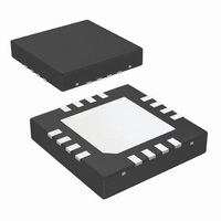
Physical Dimensions inches (millimeters) unless otherwise noted (See AN-1187 for PCB Design and Assembly Recommendations) Order Number DS25CP102QSQ NS Package Number SQA16A 15 www.national.com ...
Page 16
... For more National Semiconductor product information and proven design tools, visit the following Web sites at: Products Amplifiers www.national.com/amplifiers Audio www.national.com/audio Clock and Timing www.national.com/timing Data Converters www.national.com/adc Interface www.national.com/interface LVDS www.national.com/lvds Power Management www.national.com/power Switching Regulators www.national.com/switchers LDOs www.national.com/ldo LED Lighting www ...