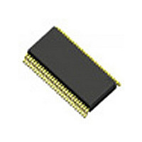
IDT74FST163233PA IDT, Integrated Device Technology Inc, IDT74FST163233PA Datasheet - Page 2

IDT74FST163233PA
Manufacturer Part Number
IDT74FST163233PA
Description
Manufacturer
IDT, Integrated Device Technology Inc
Datasheet
1.IDT74FST163233PA.pdf
(7 pages)
Specifications of IDT74FST163233PA
Logic Family
FST
Number Of Bits
32
Number Of Elements
2
Technology
CMOS
High Level Output Current
-128mA
Low Level Output Current
128mA
On Resistance
10Ohm
Propagation Delay Time
7ns
Package Type
TSSOP
Operating Temp Range
-40C to 85C
Operating Temperature Classification
Industrial
Operating Supply Voltage (min)
4.5V
Operating Supply Voltage (typ)
5V
Operating Supply Voltage (max)
5.5V
Quiescent Current
3uA
Pin Count
56
Mounting
Surface Mount
Lead Free Status / Rohs Status
Not Compliant
Available stocks
Company
Part Number
Manufacturer
Quantity
Price
Company:
Part Number:
IDT74FST163233PA
Manufacturer:
IDT
Quantity:
6 268
PIN CONFIGURATION
IDT74FST163233
16-BIT 2:1 MUX/DEMUX SWITCH
TEST
TEST
GND
1B
2B
1A
1B
2B
1A
1B
2B
1A
1B
2B
V
0A
1B
2B
0A
1B
2B
0A
1B
2B
0A
1B
2B
1A
CC
10
10
11
12
12
13
14
14
15
16
16
1
2
2
3
4
4
5
6
6
7
8
8
9
0
1
10
12
13
14
15
16
17
18
19
20
21
22
23
24
25
26
27
28
1
2
3
4
5
6
7
8
9
11
SSOP/ TSSOP
TOP VIEW
56
55
54
53
52
51
50
49
48
47
46
45
44
43
42
41
40
39
38
37
36
35
34
33
32
31
30
29
1B
2B
0A
1B
2B
0A
1B
2B
0A
1B
2B
0A
GND
V
1B
2B
1A
1B
2B
1A
1B
2B
1A
1B
2B
1A
SEL
SEL
CC
1
1
2
3
3
4
5
5
6
7
7
8
9
9
10
11
11
12
13
13
14
15
15
16
0
1
2
CAPACITANCE
ABSOLUTE MAXIMUM RATINGS
NOTES:
1. Stresses greater than those listed under ABSOLUTE MAXIMUM RATINGS may cause
2. Vcc, Control, and Switch terminals.
PIN DESCRIPTION
FUNCTION TABLE
NOTE:
1. H = HIGH Voltage Level
NOTES:
1. Capacitance is characterized but not tested.
2. T
Symbol
V
T
I
Symbol
C
C
OUT
Pin Names
STG
TERM
permanent damage to the device. This is a stress rating only and functional operation
of the device at these or any other conditions above those indicated in the operational
sections of this specification is not implied. Exposure to absolute maximum rating
conditions for extended periods may affect reliability.
L = LOW Voltage Level
X = DOn't Care
IN
I/O
A, 1B, 2B
TEST
A
SEL
= 25°C, f = 1MHz, V
(2)
SEL
SEL
0, 1
0, 1
H
H
X
X
L
L
Terminal Voltage with Respect to GND
Storage Temperature
Maximum Continuous Channel Current
0
1
Control Input Capacitance
Switch Input/Output
Capacitance
Parameter
I/O
I/O
I
Description
IN
= 0V, V
Buses A, 1B, 2B
Control Pins for MUX and Switch Enable Functions
(1)
TEST
TEST
H
H
L
L
L
L
INDUSTRIAL TEMPERATURE RANGE
OUT
0
1
A Port
B Port
(1)
= 0V.
Description
Conditions
Switch Off
Switch Off
0A to 1B and 0A to 2B
1A to 1B and 1A to 2B
–65 to +150
–0.5 to +7
Description
Description
Max
0A to 1B
0A to 2B
1A to 1B
1A to 2B
128
(2)
Typ.
(1)
17
12
6
Unit
Unit
mA
° C
pF
pF
V


