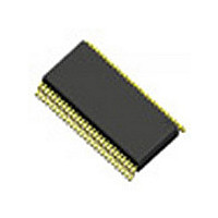
IDT74FST163233PA IDT, Integrated Device Technology Inc, IDT74FST163233PA Datasheet - Page 4

IDT74FST163233PA
Manufacturer Part Number
IDT74FST163233PA
Description
Manufacturer
IDT, Integrated Device Technology Inc
Datasheet
1.IDT74FST163233PA.pdf
(7 pages)
Specifications of IDT74FST163233PA
Logic Family
FST
Number Of Bits
32
Number Of Elements
2
Technology
CMOS
High Level Output Current
-128mA
Low Level Output Current
128mA
On Resistance
10Ohm
Propagation Delay Time
7ns
Package Type
TSSOP
Operating Temp Range
-40C to 85C
Operating Temperature Classification
Industrial
Operating Supply Voltage (min)
4.5V
Operating Supply Voltage (typ)
5V
Operating Supply Voltage (max)
5.5V
Quiescent Current
3uA
Pin Count
56
Mounting
Surface Mount
Lead Free Status / Rohs Status
Not Compliant
Available stocks
Company
Part Number
Manufacturer
Quantity
Price
Company:
Part Number:
IDT74FST163233PA
Manufacturer:
IDT
Quantity:
6 268
NOTES:
1. For conditions shown as Max. or Min., use appropriate value specified under Electrical Characteristics for the applicable device type. T
2. Typical values are at V
3. Per TTL driven input (V
4. This parameter represents the current required to switch the internal capacitance of the control inputs at the specified frequency.
5. C
6. I
POWER SUPPLY CHARACTERISTICS
IDT74FST163233
16-BIT 2:1 MUX/DEMUX SWITCH
Symbol
Switch inputs generate no significant power supply currents as they transition. This parameter is not directly testable, but is derived for use in Total Power Supply Calculations.
C
I
I
ΔI
D
N
I
f
N = Number of Control Inputs Toggling at f
C
C
CC
CCD
i
PD
PD
H
T
= Control Input Frequency
ΔI
I
I
CC
= I
= I
CCD
CCD
I
= Number of TTL Inputs at D
= Duty Cycle for TTL Inputs High
= Quiescent Current
C
CC
= I
= Power Dissipation Capacitance
QUIESCENT
CC
= Dynamic Current Caused by an Input Transition Pair (HLH or LHL)
= Power Supply Current for a TTL High Input (V
CCD
+ ΔI
/V
CC
CC
Quiescent Power Supply Current
TTL Inputs HIGH
Dynamic Power Supply
Current
Dynamic Power Supply
Current
Total Power Supply Current
+ I
D
H
INPUTS
N
T
+ I
(4,5)
(4,5)
CC
+ I
CCD
IN
= 3.4V). All other inputs at V
DYNAMIC
= 5.0V, +25°C ambient.
Parameter
(f
i
N)
H
i
(6)
IN
CC
= 3.4V)
V
V
V
One Select Pin Toggling
50% Duty Cycle
V
One Test Pin Toggling
50% Duty Cycle
V
One Select Pin Toggling
f
50% Duty Cycle
V
Two Select Pins Toggling
f
50% Duty Cycle
or GND. Switch inputs do not contribute to ΔI
i
i
IN
CC
CC
CC
CC
CC
= 10MHz
= 10MHz
= 3.4V
= Max.
= Max.
= Max.
= Max.
= Max.
(3)
Test Conditions
4
V
V
V
V
V
V
V
V
V
V
V
V
(1)
IN
IN
IN
IN
IN
IN
IN
IN
IN
IN
IN
IN
= V
= V
= V
= V
= V
= V
= 3.4V
= 3.4V
= GND
= GND
= GND
= GND
CC
CC
CC
CC
CC
CC
CC.
INDUSTRIAL TEMPERATURE RANGE
Min.
—
—
—
—
—
—
—
A
Typ.
= –40°C to +85°C
120
0.5
0.3
0.6
0.6
1.1
30
(2)
Max.
160
1.5
0.4
1.2
0.8
2.3
40
Select
MHz/
MHz/
Unit
µA/
µA/
Test
mA
mA


