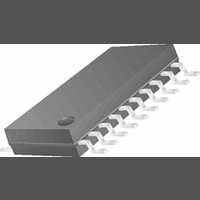
LMX2352TM National Semiconductor, LMX2352TM Datasheet - Page 17

LMX2352TM
Manufacturer Part Number
LMX2352TM
Description
07B5847
Manufacturer
National Semiconductor
Datasheet
1.LMX2352TMNOPB.pdf
(21 pages)
Specifications of LMX2352TM
Pll Type
Frequency Synthesis
Frequency
1.2GHz
Supply Current
4.75mA
Supply Voltage Range
2.7V To 5.5V
Digital Ic Case Style
TSSOP
No. Of Pins
24
Rohs Compliant
No
Available stocks
Company
Part Number
Manufacturer
Quantity
Price
Company:
Part Number:
LMX2352TM/NOPB
Manufacturer:
TI/NSC
Quantity:
1 000
Part Number:
LMX2352TMB
Manufacturer:
NS/国半
Quantity:
20 000
Company:
Part Number:
LMX2352TMX
Manufacturer:
NS/TI
Quantity:
3
Part Number:
LMX2352TMX
Manufacturer:
NS/国半
Quantity:
20 000
Company:
Part Number:
LMX2352TMX/NOPB
Manufacturer:
ST
Quantity:
7 600
Programming Description
4.4.1 Programmable CMOS Output Truth Table
When the FastLock bit is set to one, OUT_0 and OUT_1 are don’t care bits. FastLock mode utilizes the OUT0 and OUT1 output
pins to synchronously switch between active low and TRI-STATE. The OUT0 = LOW state occurs whenever the RF loop’s CP_8X
is selected HIGH while the FastLock bit is set HIGH (see programming description 3.2.2). The OUT0 pin reverts to TRI-STATE
when the CP_8X bit is LOW. Similarly for the IF loop, the synchronous activation of OUT1= LOW or TRI-STATE, is dependent on
whether the CP_GAIN_8 is high or low respectively (see programming description 3.1.4).
4.5 SERIAL DATA INPUT TIMING
Note: Data shifted into register on clock rising edge. Data is shifted in MSB first.
FastLock
TEST CONDITIONS: The Serial Data Input Timing is tested using a symmetrical waveform around Vcc/2. The test waveform has an edge rate of 0.6 V/nsec
with amplitudes of 2.2V
OUT_0
OUT_1
BIT
LOCATION
@
IF_N[17]
IF_N[18]
IF_N[20]
Vcc=2.7 V and 2.6V
@
OUT0 CMOS output pin level
OUT1 CMOS output pin level
Vcc = 5.5 V.
(Continued)
FastLock mode select
FUNCTION
set
set
17
CMOS output
LOW
LOW
0
FastLock mode
DS100831-3
HIGH
HIGH
1
www.national.com


