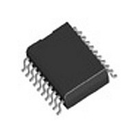
AD7801BR-REEL7 Analog Devices Inc, AD7801BR-REEL7 Datasheet - Page 4

AD7801BR-REEL7
Manufacturer Part Number
AD7801BR-REEL7
Description
Manufacturer
Analog Devices Inc
Datasheet
1.AD7801BR-REEL7.pdf
(16 pages)
Specifications of AD7801BR-REEL7
Number Of Channels
1
Resolution
8b
Conversion Rate
833KSPS
Interface Type
Parallel
Single Supply Voltage (typ)
3.3/5V
Dual Supply Voltage (typ)
Not RequiredV
Settling Time
2us
Architecture
Current Steering
Power Supply Requirement
Single
Output Type
Voltage
Integral Nonlinearity Error
±1LSB
Single Supply Voltage (min)
2.7V
Single Supply Voltage (max)
5.5V
Dual Supply Voltage (min)
Not RequiredV
Dual Supply Voltage (max)
Not RequiredV
Operating Temp Range
-40C to 105C
Operating Temperature Classification
Industrial
Mounting
Surface Mount
Pin Count
20
Package Type
SOIC W
Lead Free Status / Rohs Status
Not Compliant
AD7801
Pin
No.
1–8
9
10
11
12
13
14
15
16
17
18
19
20
Mnemonic
D7–D0
CS
WR
DGND
PD
LDAC
CLR
V
REFIN
AGND
NC
V
DGND
DD
OUT
Function
Parallel Data Inputs. 8-bit data is loaded to the input register of the AD7801 under the control of CS and WR.
Chip Select. Active low logic input.
Write Input. WR is an active low logic input used in conjunction with CS to write data to the input register.
Digital Ground
Active low input used to put the part into low power mode reducing current consumption to less than 1 A.
Load DAC Logic Input. When this logic input is taken low the DAC output is updated with the contents of
its DAC register. If LDAC is permanently tied low the DAC is updated on the rising edge of WR.
Asynchronous Clear Input (Active Low). When this input is taken low the DAC register is loaded with all
zeroes and the DAC output is cleared to zero volts.
Power Supply Input. This part can be operated from +2.7 V to +5.5 V and should be decoupled to GND.
External Reference Input. This can be used as the reference for the DAC. The range on this reference input is
1 V to V
Analog Ground reference point and return point for all analog current on the part.
No Connect Pin.
Analog Output Voltage from the DAC. The output amplifier can swing rail to rail on its output.
Digital Ground reference point and return point for all digital current on the part.
DD
/2. If REFIN is tied directly to V
PIN FUNCTION DESCRIPTIONS
(MSB) DB7
(LSB) DB0
PIN CONFIGURATION
DB6
DB5
DB4
DB3
DB2
DB1
WR
CS
10
NC = NO CONNECT
1
2
3
4
5
6
7
8
9
(Not to Scale)
–4–
TOP VIEW
AD7801
DD
the internal V
20
19
18
17
16
15
14
13
12
11
DGND
V
NC
AGND
REFIN
V
CLR
LDAC
PD
DGND
OUT
DD
DD
/2 reference is selected.
REV. 0


