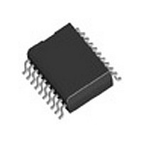
AD7801BR-REEL7 Analog Devices Inc, AD7801BR-REEL7 Datasheet - Page 8

AD7801BR-REEL7
Manufacturer Part Number
AD7801BR-REEL7
Description
Manufacturer
Analog Devices Inc
Datasheet
1.AD7801BR-REEL7.pdf
(16 pages)
Specifications of AD7801BR-REEL7
Number Of Channels
1
Resolution
8b
Conversion Rate
833KSPS
Interface Type
Parallel
Single Supply Voltage (typ)
3.3/5V
Dual Supply Voltage (typ)
Not RequiredV
Settling Time
2us
Architecture
Current Steering
Power Supply Requirement
Single
Output Type
Voltage
Integral Nonlinearity Error
±1LSB
Single Supply Voltage (min)
2.7V
Single Supply Voltage (max)
5.5V
Dual Supply Voltage (min)
Not RequiredV
Dual Supply Voltage (max)
Not RequiredV
Operating Temp Range
-40C to 105C
Operating Temperature Classification
Industrial
Mounting
Surface Mount
Pin Count
20
Package Type
SOIC W
Lead Free Status / Rohs Status
Not Compliant
AD7801
Reference
The AD7801 has the ability to use either an external reference
applied through the REFIN pin or an internal reference generated
from V
where either the internal V
can be selected.
The internal reference is selected by tying the REFIN pin to
V
applied to the REFIN pin and if this is 1 V below V
internal circuitry will select this externally applied reference as
the reference source for the DAC.
Digital Interface
The AD7801 contains a fast parallel interface allowing this
DAC to interface to industry standard microprocessors,
microcontrollers and DSP machines. There are two modes in
which this parallel interface can be configured to update the
DAC output. The synchronous update mode allows synchro-
nous updating of the DAC output; the automatic update mode
allows the DAC to be updated individually following a write
cycle. Figure 21 shows the internal logic associated with the
digital interface. The PON STRB signal is internally generated
from the power-on reset circuitry and is low during the power-
on reset phase of the power up procedure.
The AD7801 has a double buffered interface, which allows for
synchronous updating of the DAC output. Figure 22 shows a
block diagram of the register arrangement within the AD7801.
DD
PON STRB
. If an external reference is to be used, this can be directly
LDAC
DB7-DB0
CLR
WR
DD
CS
. Figure 20 shows the reference input arrangement
LDAC
CLR
WR
CS
Figure 22. Register Arrangement
Figure 21. Logic Interface
8
MLE
4
4
CONTROL LOGIC
DD
/2 or the externally applied reference
15
15
SLE
CLEAR
SET SLE
LDAC
ENABLE
15
15
DAC CONTROL
LOGIC
DD
30
30
UPPER
NIBBLE
LOWER
NIBBLE
CLR
, the
MLE
SLE
–8–
Automatic Update Mode
In this mode of operation the LDAC signal is permanently tied
low. The state of the LDAC is sampled on the rising edge of
WR. LDAC being low allows the DAC register to be automati-
cally updated on the rising edge of WR. The output update
occurs on the rising edge of WR. Figure 23 shows the timing
associated with the automatic update mode of operation and
also the status of the various registers during this frame.
Figure 23. Timing and Register Arrangement for Auto-
matic Update Mode
Synchronous Update Mode
In this mode of operation the LDAC signal is used to update the
DAC output to synchronize with other updates in the system.
The state of the LDAC is sampled on the rising edge of WR. If
LDAC is high, the automatic update mode is disabled and the
DAC latch is updated at any time after the write by taking
LDAC low. The output update occurs on the falling edge of
LDAC. LDAC must be taken back high again before the next
data transfer takes place. Figure 24 shows the timing associated
with the synchronous update mode of operation and also the
status of the various registers during this frame.
Figure 24. Timing and Register Arrangement for Synchro-
nous Update Mode
DAC REG (SLE)
DAC REG (SLE)
I/P REG (MLE)
I/P REG (MLE)
LDAC = 0
D7-D0
D7-D0
LDAC
V
V
OUT
OUT
WR
WR
CS
CS
TRACK
HOLD
HOLD
TRACK
TRACK
HOLD
HOLD
HOLD
TRACK
HOLD
TRACK
HOLD
REV. 0


