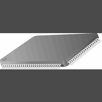
PC87393VJG National Semiconductor, PC87393VJG Datasheet - Page 66

PC87393VJG
Manufacturer Part Number
PC87393VJG
Description
IC, SUPER I/O DEVICE, TQFP-100
Manufacturer
National Semiconductor
Specifications of PC87393VJG
Data Rate
2Mbps
Supply Voltage Range
3V to 3.6V
Logic Case Style
TQFP
No. Of Pins
100
Operating Temperature Range
0°C to +70°C
Termination Type
SMD
Transceiver Type
Interface
Rohs Compliant
No
Available stocks
Company
Part Number
Manufacturer
Quantity
Price
Part Number:
PC87393VJG
Manufacturer:
NS/国半
Quantity:
20 000
www.national.com
2.0 Device Architecture and Configuration
2.19.3 X-Bus Memory Range Programming
LPC memory transactions and/or LPC-FWH transactions can be forwarded to the PC8739x X-Bus. The X-Bus Memory Con-
figuration register defines the address space to which the PC8739x responds. The XCNF2-0 strap inputs impact the default
setting of the X-Bus Memory Configuration register enable boot process from memories connected on the X-Bus. Two mem-
ory areas may be individually enabled: a user-defined zone, and BIOS memory (BIOS-LPC and/or BIOS-FWH spaces).
To enable BIOS support, set the XCNF2-0 strap inputs to select any of the BIOS modes (see Section 1.5.11 for details). The
PC8739x responds to LPC memory read and write transactions to/from the BIOS address spaces, shown in Table 29, as
long as BIOS LPC Enable (bit 0) of the X-Bus Memory Configuration register is set.
The PC8739x responds to LPC-FWH read and write transactions from/to the high memory address range (’386’ mode BIOS
range), shown in Table 29, as long as BIOS FWH Enable (bit 3) of the X-Bus Memory Configuration register is set.
Upon reset in BIOS enabled mode (XCNF 000), the BIOS LPC Enable bit is set and the BIOS FWH Enable bit is set. The
PC8739x automatically detects the type of host boot protocol in use via the first completed BIOS read operation after reset.
If the first read is an LPC memory read, the BIOS FWH Enable bit is cleared. If the first read is an LPC-FWH read, the BIOS
LPC Enable bit is cleared. Any other LPC or LPC-FWH transactions are ignored. The bits are cleared only by the first read
operation, allowing software to enable response to these address ranges by setting the bit. Figure 7 illustrates this behavior.
The User-Defined Memory Zone (UDMZ) is specified via a 32-bit start address. This address is formed by 8 bits of the X-
Bus Memory Base Address Low Byte register, 8 bits of the X-Bus Memory Base Address HIgh Byte register and 16 least
significant bits of 0. The size of the window is specified through the X-Bus Memory Size Configuration register. The zone
base address must be aligned to the block size.
The address used for the X-Bus transaction is the 28 least significant bits of the address bus. In read transactions, the data
read from the X-Bus is passed to the LPC bus. In write transactions, the data from the LPC is passed to the X-Bus.
2.19.4 X-Bus I/O Configuration Register
This register is reset by hardware to 00h.
Location:
Note:
Only hardware-controlled transitions
possible via software writes to the bits.
are shown. Other transitions are
Index F0h
Memory Address Range
000E 0000h - 000E FFFFh
000F 0000h - 000F FFFFh
FFC0 0000h - FFFFF FFFh
Memory Address Range
FFC0 0000h - FFFFF FFFh
RESET
XCNF[2-0] Disable BIOS
Table 30. BIOS-FWH Memory Space Definition
Table 29. BIOS-LPC Memory Space Definition
First LPC Memory Read
Figure 7. BIOS Mapping Enable Scheme
BIOS FWH Enable =0
BIOS LPC Enable = 1
Extended BIOS Range (Legacy)
386 mode BIOS Range.
386 mode BIOS Range.
Only when Extended BIOS Enable bit in X-Bus Memory
Range Configuration register is set
BIOS Range (Legacy)
This is the upper 4 Mbyte of the memory space
This is the upper 4 Mbyte of the memory space
66
(Continued)
BIOS FWH Enable =1
BIOS LPC Enable = 1
BIOS FWH Enable =0
BIOS LPC Enable = 0
Description
Description
BIOS FWH Enable =1
BIOS LPC Enable = 0
First LPC FWH Read


