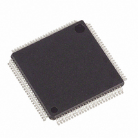
DS21354LN+ Maxim Integrated Products, DS21354LN+ Datasheet - Page 30

DS21354LN+
Manufacturer Part Number
DS21354LN+
Description
IC TXRX E1 1-CHIP 3.3V 100-LQFP
Manufacturer
Maxim Integrated Products
Datasheet
1.DS2154LNA2.pdf
(124 pages)
Specifications of DS21354LN+
Function
Single-Chip Transceiver
Interface
E1, HDLC
Number Of Circuits
1
Voltage - Supply
3.14 V ~ 3.47 V
Current - Supply
75mA
Operating Temperature
-40°C ~ 85°C
Mounting Type
Surface Mount
Package / Case
100-LQFP
Includes
Remote and AIS Alarm Detector / Generator
Lead Free Status / RoHS Status
Lead free / RoHS Compliant
Power (watts)
-
- Current page: 30 of 124
- Download datasheet (945Kb)
5. CONTROL, ID, AND TEST REGISTERS
The operation of the DS21354/DS21554 is configured via a set of 10 control registers. Typically, the
control registers are only accessed when the system is first powered up. Once the device has been
initialized, the control registers need only to be accessed when there is a change in the system
configuration. There are two receive control registers (RCR1 and RCR2), two transmit control registers
(TCR1 and TCR2), and six common control registers (CCR1 to CCR6). Each of the 10 registers is
described in this section.
There is a device identification register (IDR) at address 0Fh. The MSB of this read-only register is fixed
to a one, indicating that an E1 SCT is present. The next three MSBs are used to indicate which E1 device
is present—DS2154, DS21354, or DS21554. The T1 pin-for-pin compatible SCTs have a logic zero in
the MSB position with the following three MSBs indicating which T1 SCT is present—DS2152,
DS21352, or DS21552.
Table 5-1. Device ID Bit Map
The lower four bits of the IDR are used to display the die revision of the chip. The test registers at
addresses 09, 15, 19, and AC hex are used by the factory in testing the DS21354/DS21554. On power-up,
the test registers should be set to 00h in order for the DS21354/DS21554 to operate properly. Certain bits
of TEST3 are used to select monitor mode functions. Please see Section
5.1.
On power-up, after the supplies are stable the DS21354/DS21554 should be configured for operation by
writing to all the internal registers (this includes setting the test registers to 00h) since the contents of the
internal registers cannot be predicted on power-up. The LIRST (CCR5.7) should be toggled from zero to
one to reset the line-interface circuitry (it will take the device about 40ms to recover from the LIRST bit
being toggled). Finally, after the TSYSCLK and RSYSCLK inputs are stable, the ESR bits (CCR6.0 and
CCR6.1) should be toggled from a zero to a one (this step can be skipped if the elastic stores are
disabled).
DS21352
DS21552
DS21354
DS21554
DS2152
DS2154
Power-Up Sequence
SCT
Table 5-1
T1/E1
0
0
0
1
1
1
represents the possible variations of these bits and the associated SCT.
BIT 6
30 of 124
0
0
0
0
0
0
BIT 5
0
0
1
0
0
1
15.5
for further details.
BIT 4
0
1
0
0
1
0
Related parts for DS21354LN+
Image
Part Number
Description
Manufacturer
Datasheet
Request
R

Part Number:
Description:
Manufacturer:
Maxim Integrated Products
Datasheet:

Part Number:
Description:
power light source Luxeon Line
Manufacturer:
LUMILEDS [Lumileds Lighting Company]
Datasheet:

Part Number:
Description:
MAX7528KCWPMaxim Integrated Products [CMOS Dual 8-Bit Buffered Multiplying DACs]
Manufacturer:
Maxim Integrated Products
Datasheet:

Part Number:
Description:
Single +5V, fully integrated, 1.25Gbps laser diode driver.
Manufacturer:
Maxim Integrated Products
Datasheet:

Part Number:
Description:
Single +5V, fully integrated, 155Mbps laser diode driver.
Manufacturer:
Maxim Integrated Products
Datasheet:

Part Number:
Description:
VRD11/VRD10, K8 Rev F 2/3/4-Phase PWM Controllers with Integrated Dual MOSFET Drivers
Manufacturer:
Maxim Integrated Products
Datasheet:

Part Number:
Description:
Highly Integrated Level 2 SMBus Battery Chargers
Manufacturer:
Maxim Integrated Products
Datasheet:

Part Number:
Description:
Current Monitor and Accumulator with Integrated Sense Resistor; ; Temperature Range: -40°C to +85°C
Manufacturer:
Maxim Integrated Products

Part Number:
Description:
TSSOP 14/A°/RS-485 Transceivers with Integrated 100O/120O Termination Resis
Manufacturer:
Maxim Integrated Products

Part Number:
Description:
TSSOP 14/A°/RS-485 Transceivers with Integrated 100O/120O Termination Resis
Manufacturer:
Maxim Integrated Products

Part Number:
Description:
QFN 16/A°/AC-DC and DC-DC Peak-Current-Mode Converters with Integrated Step
Manufacturer:
Maxim Integrated Products

Part Number:
Description:
TDFN/A/65V, 1A, 600KHZ, SYNCHRONOUS STEP-DOWN REGULATOR WITH INTEGRATED SWI
Manufacturer:
Maxim Integrated Products

Part Number:
Description:
Integrated Temperature Controller f
Manufacturer:
Maxim Integrated Products

Part Number:
Description:
SOT23-6/I°/45MHz to 650MHz, Integrated IF VCOs with Differential Output
Manufacturer:
Maxim Integrated Products


