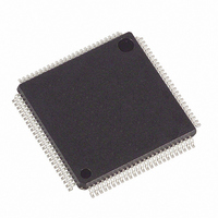
DS21354LN+ Maxim Integrated Products, DS21354LN+ Datasheet - Page 58

DS21354LN+
Manufacturer Part Number
DS21354LN+
Description
IC TXRX E1 1-CHIP 3.3V 100-LQFP
Manufacturer
Maxim Integrated Products
Datasheet
1.DS2154LNA2.pdf
(124 pages)
Specifications of DS21354LN+
Function
Single-Chip Transceiver
Interface
E1, HDLC
Number Of Circuits
1
Voltage - Supply
3.14 V ~ 3.47 V
Current - Supply
75mA
Operating Temperature
-40°C ~ 85°C
Mounting Type
Surface Mount
Package / Case
100-LQFP
Includes
Remote and AIS Alarm Detector / Generator
Lead Free Status / RoHS Status
Lead free / RoHS Compliant
Power (watts)
-
DS21354/DS21554 3.3V/5V E1 Single-Chip Transceivers
the TSRs before the old data is retransmitted. ITU specifications recommend that the ABCD signaling not
be set to all zeros because they will emulate a CAS multiframe alignment word.
The TS1 register is special because it contains the CAS multiframe alignment word in its upper nibble.
The upper nibble must always be set to 0000 or else the terminal at the far end loses multiframe
synchronization. If the user wishes to transmit a multiframe alarm to the far end, then the TS1.2 bit
should be set to one. If no alarm is to be transmitted, then the TS1.2 bit should be cleared. The three
remaining bits in TS1 are the spare bits. If they are not used, they should be set to one. In CCS signaling
mode, TS1 to TS16 can also be used to insert signaling information. Via the SR2.5 bit, the user will be
informed when the signaling registers need to be loaded with data. The user has 2ms to load the data
before the old data will be retransmitted.
Via the CCR3.6 bit, the user has the option to use the Transmit Channel Blocking Registers (TCBRs) to
determine on a channel by channel basis, which signaling bits are to be inserted via the TSRs (the
corresponding bit in the TCBRs = 1) and which are to be sourced from the TSER or TSIG pin (the
corresponding bit in the TCBRs = 0). See
Figure 18-15
for more details.
Hardware-Based Signaling
9.2.
9.2.1.
Receive Side
In the receive side of the hardware-based signaling, there are two operating modes for the signaling
buffer—signaling extraction and signaling reinsertion. Signaling extraction involves pulling the signaling
bits from the receive data stream and buffering them over a four-multiframe buffer and outputting them in
a serial PCM fashion on a channel-by-channel basis at the RSIG output. This mode is always enabled. In
this mode, the receive elastic store may be enabled or disabled. If the receive elastic store is enabled, then
the backplane clock (RSYSCLK) must be 2.048MHz/4.096MHz/8.192MHz. The ABCD signaling bits
are output on RSIG in the lower nibble of each channel. The RSIG data is updated once a multiframe
(2ms) unless a freeze is in effect. See the timing diagrams in Section
18.1
for some examples.
The other hardware-based signaling operating mode called signaling reinsertion can be invoked by setting
the RSRE control bit high (CCR3.3 = 1). In this mode, the user provides a multiframe sync at the RSYNC
pin and the signaling data is realigned at the RSER output according to this applied multiframe boundary.
In this mode, the elastic store must be enabled and the backplane clock must be
2.048MHz/4.096MHz/8.192MHz.
The signaling data in the two-multiframe buffer is frozen in a known good state upon either a loss of
synchronization (OOF event), carrier loss, or frame slip. To allow this freeze action to occur, the RFE
control bit (CCR2.0) should be set high. The user can force a freeze by setting the RFF control bit
(CCR2.1) high. Setting the RFF bit high causes the same freezing action as if a loss of synchronization,
carrier loss, or slip has occurred.
The two-multiframe buffer provides an approximate one-multiframe delay in the signaling bits provided
at the RSIG pin (and at the RSER pin if RSRE = 1 via CCR3.3). When freezing is enabled (RFE = 1), the
signaling data is held in the last known good state until the corrupting error condition subsides. When the
error condition subsides, the signaling data is held in the old state for an additional 3ms to 5ms before
being allowed to be updated with new signaling data.
58 of 124


