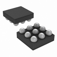
LM4670ITLX/NOPB National Semiconductor, LM4670ITLX/NOPB Datasheet - Page 3

LM4670ITLX/NOPB
Manufacturer Part Number
LM4670ITLX/NOPB
Description
IC AMP AUDIO PWR 3W MONO D 9USMD
Manufacturer
National Semiconductor
Series
Boomer®r
Type
Class Dr
Datasheet
1.LM4670ITLXNOPB.pdf
(20 pages)
Specifications of LM4670ITLX/NOPB
Output Type
1-Channel (Mono)
Max Output Power X Channels @ Load
3W x 1 @ 4 Ohm
Voltage - Supply
2.4 V ~ 5.5 V
Features
Depop, Differential Inputs, Short-Circuit Protection, Shutdown
Mounting Type
Surface Mount
Package / Case
9-MicroBump
Lead Free Status / RoHS Status
Lead free / RoHS Compliant
Other names
LM4670ITLX/NOPBTR
|V
PSRR
CMRR
|I
|I
I
I
V
V
R
A
R
P
DD
SD
Symbol
IH
IL
SDIH
SDIL
V
O
OSD
SD
Absolute Maximum Ratings
If Military/Aerospace specified devices are required,
please contact the National Semiconductor Sales Office/
Distributors for availability and specifications.
Electrical Characteristics
The following specifications apply for A
ply for T
OS
|
Supply Voltage (Note 1)
Storage Temperature
Voltage at Any Input Pin
Power Dissipation (Note 3)
ESD Susceptibility (Note 4)
ESD Susceptibility (Note 5)
Junction Temperature (T
Thermal Resistance
|
|
GSM
GSM
A
Differential Output Offset Voltage
GSM Power Supply Rejection Ratio
GSM Common Mode Rejection
Ratio
Logic High Input Current
Logic Low Input Current
Quiescent Power Supply Current
Shutdown Current (Note 9)
Shutdown voltage input high
Shutdown voltage input low
Output Impedance
Gain
Resistance from Shutdown Pin to
GND
Output Power (Notes 11,12)
= 25˚C.
Parameter
JMAX
V
)
DD
+ 0.3V ≥ V ≥ GND - 0.3V
V
= 2V/V (R
Internally Limited
−65˚C to +150˚C
(Notes 1, 2)
V
V
V
Input Referred
V
V
V
Input Referred
V
V
V
V
V
V
V
V
R
THD = 10% (max)
f = 1kHz, 22kHz BW
V
V
V
R
THD+N = 1% (max)
f = 1kHz, 22kHz BW
V
V
V
(Notes 1, 2)
I
DD
DD
DD
IC
IC
DD
DD
IN
IN
IN
SHUTDOWN
DD
SHUTDOWN
L
DD
DD
DD
L
DD
DD
DD
= 0V, A
= 15µH + 4Ω + 15µH,
= 15µH + 4Ω + 15µH,
= V
= V
= 0V, No Load, V
= 0V, No Load, V
= 0V, No Load, V
I
= 2.4V to 5.0V
= 2.4V to 5.0V,
= 2.4V to 5.0V
= 5.0V, V
= 5.0V, V
= 2.4V to 5.0V
= 5V
= 3.6V
= 2.5V
= 5V,
= 3.6V,
= 2.5V,
= 150kΩ), R
150˚C
2.0kV
DD
DD
200V
6.0V
/2 to 0.5V,
/2 to V
V
Conditions
= 2V/V,
= 0V
= 0.4V
I
I
= 5.8V
= –0.3V
3
DD
L
= 15µH + 8Ω + 15µH unless otherwise specified. Limits ap-
– 0.8V,
Operating Ratings
Soldering Information
See AN-1112 "microSMD Wafers Level Chip Scale
Package."
Temperature Range
Supply Voltage (Note 12)
DD
DD
DD
θ
θ
T
JA
JA
MIN
= 5.0V
= 3.6V
= 2.4V
(micro SMD)
(LLP)
≤ T
A
≤ T
MAX
300kΩ/R
(Note 6)
Typical
>
0.01
300
675
550
7.0
4.8
3.8
1.0
0.8
3.0
1.5
2.3
1.2
64
80
20
100
1
LM4670
I
(Note 1) (Note 2)
(Notes 7, 8)
270kΩ/R
330kΩ/R
Limit
100
1.4
0.4
25
10
5
5
1
−40˚C ≤ T
2.4V ≤ V
I
I
www.national.com
V/V (max)
mV (max)
mA (max)
mA (max)
V/V (min)
µA (max)
µA (max)
µA (max)
DD
(Limits)
V (max)
V (min)
220˚C/W
A
Units
73˚C/W
mW
mW
mA
≤ 85˚C
kΩ
kΩ
dB
dB
≤ 5.5V
W
W
W
W


