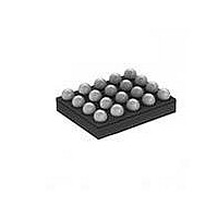
MAX97002EWP+T Maxim Integrated Products, MAX97002EWP+T Datasheet - Page 31

MAX97002EWP+T
Manufacturer Part Number
MAX97002EWP+T
Description
IC AUDIO SUBSYSTEM 20WLP
Manufacturer
Maxim Integrated Products
Series
DirectDrive™r
Type
Class Dr
Datasheet
1.MAX97002EWPT.pdf
(37 pages)
Specifications of MAX97002EWP+T
Output Type
1-Channel (Mono) with Stereo Headphones
Max Output Power X Channels @ Load
920mW x 1 @ 8 Ohm; 37mW x 2 @ 16 Ohm
Voltage - Supply
2.7 V ~ 5.5 V
Features
Depop, Differential Inputs, I²C, Mute, Shutdown, Volume Control
Mounting Type
Surface Mount
Package / Case
20-WLP
Product
Class-D
Output Power
700 mW
Available Set Gain
12 dB
Common Mode Rejection Ratio (min)
32 dB to 55 dB
Thd Plus Noise
0.05 %
Operating Supply Voltage
2.7 V to 5.5 V
Supply Current
0.32 mA to 1.85 mA
Maximum Power Dissipation
1040 mW
Maximum Operating Temperature
+ 80 C
Mounting Style
SMD/SMT
Audio Load Resistance
41.2 KOhms
Input Signal Type
Differential or Single
Minimum Operating Temperature
- 40 C
Output Signal Type
Differential
Supply Voltage (max)
5.5 V
Supply Voltage (min)
2.7 V
Lead Free Status / RoHS Status
Lead free / RoHS Compliant
Other names
MAX97002EWP+T
The MAX97002 recognizes a STOP (P) condition at any
point during data transmission except if the STOP condi-
tion occurs in the same high pulse as a START (S) condi-
tion. For proper operation, do not send a STOP condition
during the same SCL high pulse as the START condition.
The slave address is defined as the seven most sig-
nificant bits (MSBs) followed by the read/write bit. For
the MAX97002 the 7 MSBs are 1001101. Setting the
read/write bit to 1 (slave address = 0x9B) configures the
MAX97002 for read mode. Setting the read/write bit to 0
(slave address = 0x9A) configures the MAX97002 for write
mode. The address is the first byte of information sent to
the MAX97002 after the START condition.
The acknowledge bit (ACK) is a clocked 9th bit that
the MAX97002 uses to handshake receipt each byte
of data when in write mode (Figure 9). The MAX97002
pulls down SDA during the entire master-generated 9th
clock pulse if the previous byte is successfully received.
Monitoring ACK allows for detection of unsuccessful
data transfers. An unsuccessful data transfer occurs
if a receiving device is busy or if a system fault has
occurred. In the event of an unsuccessful data transfer,
the bus master retries communication. The master pulls
down SDA during the 9th clock cycle to acknowledge
receipt of data when the MAX97002 is in read mode. An
acknowledge is sent by the master after each read byte
to allow data transfer to continue. A not-acknowledge is
Figure 9. Acknowledge
Speaker and Class H Headphone Amplifiers
Audio Subsystem with Mono Class D
SDA
SCL
CONDITION
Early STOP Conditions
START
Slave Address
Acknowledge
1
28
NOT ACKNOWLEDGE
sent when the master reads the final byte of data from
the MAX97002, followed by a STOP condition.
A write to the MAX97002 includes transmission of a
START condition, the slave address with the R/W bit set
to 0, one byte of data to configure the internal register
address pointer, one or more bytes of data, and a STOP
condition. Figure 10 illustrates the proper frame format
for writing one byte of data to the MAX97002. Figure 11
illustrates the frame format for writing n-bytes of data to
the MAX97002.
The slave address with the R/W bit set to 0 indicates that
the master intends to write data to the MAX97002. The
MAX97002 acknowledges receipt of the address byte
during the master-generated 9th SCL pulse.
The second byte transmitted from the master configures
the MAX97002’s internal register address pointer. The
pointer tells the MAX97002 where to write the next byte
of data. An acknowledge pulse is sent by the MAX97002
upon receipt of the address pointer data.
The third byte sent to the MAX97002 contains the
data that is written to the chosen register. An acknowl-
edge pulse from the MAX97002 signals receipt of the
data byte. The address pointer autoincrements to the
next register address after each received data byte.
This autoincrement feature allows a master to write to
sequential registers within one continuous frame. The
master signals the end of transmission by issuing a
STOP condition. Register addresses greater than 0x09
are reserved. Do not write to these addresses.
ACKNOWLEDGE
ACKNOWLEDGMENT
CLOCK PULSE FOR
9
Write Data Format
31


