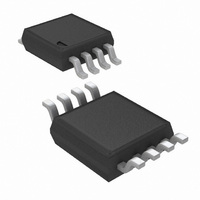
LM4902MM/NOPB National Semiconductor, LM4902MM/NOPB Datasheet

LM4902MM/NOPB
Specifications of LM4902MM/NOPB
LM4902MMTR
Available stocks
Related parts for LM4902MM/NOPB
LM4902MM/NOPB Summary of contents
Page 1
... THD+N at 1kHz for 265mW continuous average output power into 3.3V DD Typical Application FIGURE 1. Typical Audio Amplifier Application Circuit Boomer ® registered trademark of National Semiconductor Corporation. © 2002 National Semiconductor Corporation j THD+N at 1kHz for 675mW continuous average output power into Shutdown current ...
Page 2
Connection Diagrams MSOP Top View Order Number LM4902MM See NS Package Number MUA08A LLP Top View Order Number LM4902LD See NS Package Number LDA08B www.national.com 20029802 20029875 2 MSOP Marking 20029878 Top View G - Boomer Family C3 - LM4902MM ...
Page 3
... Absolute Maximum Ratings If Military/Aerospace specified devices are required, please contact the National Semiconductor Sales Office/ Distributors for availability and specifications. Supply Voltage Storage Temperature Input Voltage Power Dissipation (Note 3) ESD Susceptibility (Note 4) ESD Susceptibility (Note 5) Junction Temperature Soldering Information Small Outline Package Vapor Phase (60 sec ...
Page 4
Electrical Characteristics The following specifications apply for V 25˚C Symbol Parameter I Quiescent Power Supply Current DD I Shutdown Current SD V Output Offset Voltage OS P Output Power O THD+N Total Harmonic Distortion+Noise PSRR Power Supply Rejection Ratio Note ...
Page 5
External Components Description (Figure 1) Components 1. R Inverting input resistance which sets the closed-loop gain in conjunction with R i high pass filter with Input coupling capacitor which blocks the DC voltage at the amplifier’s input ...
Page 6
Typical Performance Characteristics THD+N vs Frequency THD+N vs Frequency THD+N vs Frequency www.national.com (Continued) THD+N vs Frequency 20029834 THD+N vs Frequency 20029836 THD+N vs Frequency 20029838 6 20029835 20029837 20029839 ...
Page 7
Typical Performance Characteristics THD+N vs Frequency THD+N vs Output Power THD+N vs Output Power (Continued) THD+N vs Output Power 20029840 THD+N vs Output Power 20029842 THD+N vs Output Power 20029844 7 20029841 20029843 20029845 www.national.com ...
Page 8
Typical Performance Characteristics THD+N vs Output Power THD+N vs Output Power THD+N vs Output Power www.national.com (Continued) THD+N vs Output Power 20029846 THD+N vs Output Power 20029848 THD+N vs Output Power 20029850 8 20029847 20029849 20029851 ...
Page 9
Typical Performance Characteristics Output Power vs Supply Voltage Output Power vs Supply Voltage Output Power vs Load Resistance (Continued) Output Power vs Supply Voltage 20029852 Output Power vs Supply Voltage 20029854 Power Dissipation vs Output Power 20029856 9 20029853 20029855 ...
Page 10
Typical Performance Characteristics Power Dissipation vs Output Power Clipping Voltage vs Supply Voltage Noise Floor www.national.com (Continued) Power Dissipation vs Output Power 20029858 Noise Floor 20029860 Frequency Response vs Input Capacitor Size 20029862 10 20029859 20029861 20029871 ...
Page 11
Typical Performance Characteristics Power Supply Rejection Ratio Power Supply Rejection Ratio Power Supply Rejection Ratio vs Supply Voltage (Continued) Power Supply Rejection Ratio 20029863 Power Supply Rejection Ratio 20029865 Power Supply Rejection Ratio vs Supply Voltage 20029867 11 20029864 20029866 ...
Page 12
Typical Performance Characteristics Power Derating Curve Open Loop Frequency Response Note 12: This curve shows the LM4902LD’s thermal dissipation ability at different ambient temperatures given the exposed-DAP of the part is soldered to a plane of 1oz. Cu with an ...
Page 13
... Further detailed and specific informa- tion concerning PCB layout, fabrication, and mounting an LD (LLP) package is available from National Semiconductor’s Package Engineering Group under application note AN1187. BRIDGE CONFIGURATION EXPLANATION ...
Page 14
Application Information Typical applications employ a 5V regulator with 10µF and a 0.1µF bypass capacitors which aid in supply stability, but do not eliminate the need for bypassing the supply nodes of the LM4902. The selection of bypass capacitors, especially ...
Page 15
Application Information ( From Equation 5, the minimum A is 1.55; use A VD Since the desired input impedance was and with ratio of ...
Page 16
Application Information DIFFERENTIAL AMPLIFIER CONFIGURATION FOR LM4902 www.national.com (Continued) 16 20029874 ...
Page 17
Physical Dimensions inches (millimeters) unless otherwise noted 8-Lead (0.118" Wide) Molded Mini Small Outline Package Order Number LM4902MM NS Package Number MUA08A 17 www.national.com ...
Page 18
... NATIONAL’S PRODUCTS ARE NOT AUTHORIZED FOR USE AS CRITICAL COMPONENTS IN LIFE SUPPORT DEVICES OR SYSTEMS WITHOUT THE EXPRESS WRITTEN APPROVAL OF THE PRESIDENT AND GENERAL COUNSEL OF NATIONAL SEMICONDUCTOR CORPORATION. As used herein: 1. Life support devices or systems are devices or systems which, (a) are intended for surgical implant ...


