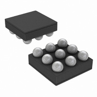
LM4670ITL/NOPB National Semiconductor, LM4670ITL/NOPB Datasheet - Page 5

LM4670ITL/NOPB
Manufacturer Part Number
LM4670ITL/NOPB
Description
IC AMP AUDIO PWR 3W MONO D 9USMD
Manufacturer
National Semiconductor
Series
Boomer®r
Type
Class Dr
Datasheet
1.LM4670ITLXNOPB.pdf
(20 pages)
Specifications of LM4670ITL/NOPB
Output Type
1-Channel (Mono)
Max Output Power X Channels @ Load
3W x 1 @ 4 Ohm
Voltage - Supply
2.4 V ~ 5.5 V
Features
Depop, Differential Inputs, Short-Circuit Protection, Shutdown
Mounting Type
Surface Mount
Package / Case
9-MicroSMD
Lead Free Status / RoHS Status
Lead free / RoHS Compliant
Other names
Q2301166
Note 1: All voltages are measured with respect to the ground pin, unless otherwise specified.
Note 2: Absolute Maximum Ratings indicate limits beyond which damage to the device may occur. Operating Ratings indicate conditions for which the device is
functional, but do not guarantee specific performance limits. Electrical Characteristics state DC and AC electrical specifications under particular test conditions which
guarantee specific performance limits. This assumes that the device is within the Operating Ratings. Specifications are not guaranteed for parameters where no limit
is given, however, the typical value is a good indication of device performance.
Note 3: The maximum power dissipation must be derated at elevated temperatures and is dictated by T
allowable power dissipation is P
The typical θ
Note 4: Human body model, 100pF discharged through a 1.5kΩ resistor.
Note 5: Machine Model, 220pF – 240pF discharged through all pins.
Note 6: Typical specifications are specified at 25˚C and represent the parametric norm.
Note 7: Tested limits are guaranteed to National’s AOQL (Average Outgoing Quality Level).
Note 8: Datasheet min/max specification limits are guaranteed by design, test, or statistical analysis.
Note 9: Shutdown current is measured in a normal room environment. Exposure to direct sunlight will increase I
be driven as close as possible to GND for minimal shutdown current. See the Application Information section under SHUTDOWN FUNCTION for more information.
Note 10: The performance graphs were taken using the Audio Precision AUX-0025 Switching Amplifier Measurement Filter in series with the LC filter on the board.
Note 11: Typical output power numbers are for the LM4670 in the ITL (µSMD) package. In the LLP (SDA) package, the output power will be lower due to higher
resistance seen from the IC output pad to PCB trace. The difference increases with lower impedance loads.
Note 12: The maximum operating voltage for the LM4670 in the SDA (LLP) package when driving 4Ω loads to greater than 10% THD+N is 5.0V.
External Components Description
(Figure 1)
Components
1.
2.
JA
is 220˚C/W for the microSMD package and 64˚C/W for the LLP package.
C
R
S
I
Supply bypass capacitor which provides power supply filtering. Refer to the Power Supply Bypassing
section for information concerning proper placement and selection of the supply bypass capacitor.
Gain setting resistor. Differential gain is set by the equation A
DMAX
= (T
JMAX
–T
A
)/θ
JA
or the number given in Absolute Maximum Ratings, whichever is lower. For the LM4670, T
Functional Description
5
JMAX
V
= 2 * 150kΩ / R
, θ
JA
SD
, and the ambient temperature T
by a maximum of 2µA. The Shutdown pin should
i
(V/V).
A
. The maximum
www.national.com
JMAX
= 150˚C.


