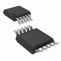
LM4929MM/NOPB National Semiconductor, LM4929MM/NOPB Datasheet

LM4929MM/NOPB
Specifications of LM4929MM/NOPB
LM4929MMTR
Related parts for LM4929MM/NOPB
LM4929MM/NOPB Summary of contents
Page 1
... The LM4929 is unity gain stable and may be configured with external gain-setting resistors. Block Diagram Boomer ® registered trademark of National Semiconductor Corporation. © 2004 National Semiconductor Corporation Key Specifications j PSRR at 217Hz and 1kHz j Output Power at 1kHz with V 1% THD+N into a 16Ω ...
Page 2
Typical Application FIGURE 2. Typical OCL Output Configuration Circuit Connection Diagram www.national.com MSOP Package 20132428 Top View (Note 10) Order Number LM4929MM See NS Package Number MUB10A 2 20132481 ...
Page 3
... Absolute Maximum Ratings If Military/Aerospace specified devices are required, please contact the National Semiconductor Sales Office/ Distributors for availability and specifications. Supply Voltage Storage Temperature Input Voltage Power Dissipation (Note 3) ESD Susceptibility (Note 4) ESD Susceptibility (Note 5) Electrical Characteristics V The following specifications apply for V 25˚ ...
Page 4
Electrical Characteristics V The following specifications apply for V 25˚C. Pin 3 connected to GND. Symbol Parameter V Output Noise Voltage NO PSRR Power Supply Rejection Ratio T Wake Up Time from Shutdown WU Note 1: All voltages are measured ...
Page 5
Typical Performance Characteristics THD+N vs Frequency THD+N vs Frequency THD+N vs Frequency THD+N vs Frequency 20132482 THD+N vs Frequency 20132406 THD+N vs Frequency 20132405 5 20132483 20132403 20132404 www.national.com ...
Page 6
Typical Performance Characteristics THD+N vs Output Power Output Power vs Load Resistance Output Power vs Supply Voltage www.national.com (Continued) THD+N vs Output Power 20132492 Output Power vs Supply Voltage 20132413 Output Power vs Load Resistance 20132495 6 20132493 20132494 20132497 ...
Page 7
Typical Performance Characteristics Power Supply Rejection Ratio Frequency Response vs Input Capacitor Size Supply Voltage vs Supply Current (Continued) Power Supply Rejection Ratio 201324A5 Open Loop Frequency Response 20132426 20132424 7 201324A6 201324A7 Clipping Voltage vs Supply Voltage 20132425 www.national.com ...
Page 8
Typical Performance Characteristics Shutdown Hysteresis Voltage, V Power Dissipation vs Output Power Power Dissipation vs Output Power V = 2.4V DD www.national.com (Continued Shutdown Hysteresis Voltage 201324B1 Power Dissipation vs Output Power ...
Page 9
Typical Performance Characteristics THD+N vs Output Power V = 2.4V 32Ω THD+N vs Output Power V = 2.4V 16Ω (Continued) THD+N vs Output Power V DD 20132438 Power Derating Curve 20132440 9 ...
Page 10
Application Information AMPLIFIER CONFIGURATION EXPLANATION As shown in Figure 1, the LM4929 has three operational amplifiers internally. Two of the amplifier’s have externally configurable gain while the other amplifier is internally fixed at the bias point acting as a unity-gain ...
Page 11
Application Information The switch and resistor guarantee that the SHUTDOWN pin will not float. This prevents unwanted state changes system with a microprocessor or microcontroller, use a digi- tal output to apply the control voltage to the SHUTDOWN ...
Page 12
Application Information determined based on the tradeoff between the amount of noise suppression that may be needed and minimizing the additional current drawn by the resistor (25mA for a 100Ω resistor and a 5V supply). ESD PROTECTION As stated in ...
Page 13
... BANNED SUBSTANCE COMPLIANCE National Semiconductor certifies that the products and packing materials meet the provisions of the Customer Products Stewardship Specification (CSP-9-111C2) and the Banned Substances and Materials of Interest Specification (CSP-9-111S2) and contain no ‘‘Banned Substances’’ as defined in CSP-9-111S2. ...


