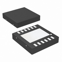
LM4854LD/NOPB National Semiconductor, LM4854LD/NOPB Datasheet - Page 19

LM4854LD/NOPB
Manufacturer Part Number
LM4854LD/NOPB
Description
IC AMP AUDIO PWR 2.3W MONO 14LLP
Manufacturer
National Semiconductor
Series
Boomer®r
Type
Class ABr
Datasheet
1.LM4854MTXNOPB.pdf
(29 pages)
Specifications of LM4854LD/NOPB
Output Type
1-Channel (Mono) with Stereo Headphones
Max Output Power X Channels @ Load
2.3W x 1 @ 3.2 Ohm; 200mW x 2 @ 16 Ohm
Voltage - Supply
2.4 V ~ 5.5 V
Features
Depop, Shutdown, Standby, Thermal Protection
Mounting Type
Surface Mount
Package / Case
14-LLP
Lead Free Status / RoHS Status
Lead free / RoHS Compliant
Other names
*LM4854LD
LM4854LD
LM4854LDNOPB
LM4854LDNOPBTR
LM4854LDNOPBTR
LM4854LDTR
LM4854LD
LM4854LDNOPB
LM4854LDNOPBTR
LM4854LDNOPBTR
LM4854LDTR
Application Information
the amplifier that drives the headphone jack’s sleeve. If this
current exceeds 500mA
EXPOSED-DAP MOUNTING CONSIDERATIONS
The LM4854’s exposed-DAP (die attach paddle) package
(LD) provides a low thermal resistance between the die and
the PCB to which the part is mounted and soldered. This
allows rapid heat transfer from the die to the surrounding
PCB copper area heatsink, copper traces, ground plane, and
finally, surrounding air. The result is a low voltage audio
power amplifier that produces 1.7W dissipation in a 4Ω load
at ≤ 1% THD+N and over 1.9W in a 3Ω load at 10% THD+N.
This high power is achieved through careful consideration of
necessary thermal design. Failing to optimize thermal design
may compromise the LM4854’s high power performance and
activate unwanted, though necessary, thermal shutdown
protection.
The LD package must have its DAP soldered to a copper
pad on the PCB. The DAP’s PCB copper pad is then, ideally,
connected to a large plane of continuous unbroken copper.
This plane forms a thermal mass, heat sink, and radiation
area. Place the heat sink area on either outside plane in the
case of a two-sided or multi-layer PCB. (The heat sink area
can also be placed on an inner layer of a multi-layer board.
The thermal resistance, however, will be higher.) Connect
the DAP copper pad to the inner layer or backside copper
PK
, the amplifier is shutdown, pro-
FIGURE 2. Typical Audio Amplifier Application Circuit
(Continued)
19
tecting the LM4854 and the external equipment. For more
information, see the section titled ’Single-Ended Output
Power Performance and Measurement Considerations’.
heat sink area with 6 (3 X 2) (LD) vias. The via diameter
should be 0.012in - 0.013in with a 1.27mm pitch. Ensure
efficient thermal conductivity by plugging and tenting the vias
with plating and solder mask, respectively.
Best thermal performance is achieved with the largest prac-
tical copper heat sink area. If the heatsink and amplifier
share the same PCB layer, a nominal 2.5in
necessary for 5V operation with a 4Ω load. Heatsink areas
not placed on the same PCB layer as the LM4854 should be
5in
The last two area recommendations apply for 25˚C ambient
temperature. Increase the area to compensate for ambient
temperatures above 25˚C. In all circumstances and under all
conditions, the junction temperature must be held below
150˚C to prevent activating the LM4854’s thermal shutdown
protection. The LM4854’s power de-rating curve in the Typi-
cal Performance Characteristics shows the maximum
power dissipation versus temperature. Example PCB layouts
for the exposed-DAP TSSOP and LD packages are shown in
the Demonstration Board Layout section. Further detailed
and specific information concerning PCB layout and fabrica-
tion and mounting an LD (LLP) is found in National Semi-
conductor’s AN1187.
2
(min) for the same supply voltage and load resistance.
2
(min) area is
www.national.com
20038207


