LM4852LQ/NOPB National Semiconductor, LM4852LQ/NOPB Datasheet - Page 6
LM4852LQ/NOPB
Manufacturer Part Number
LM4852LQ/NOPB
Description
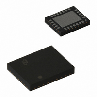
IC AMP AUDIO PWR 1.5W MONO 24LLP
Manufacturer
National Semiconductor
Series
Boomer®r
Type
Class ABr
Datasheet
1.LM4852ITLNOPB.pdf
(21 pages)
Specifications of LM4852LQ/NOPB
Output Type
1-Channel (Mono) with Stereo Headphones
Max Output Power X Channels @ Load
1.5W x 1 @ 4 Ohm; 60mW x 2 @ 32 Ohm
Voltage - Supply
2.6 V ~ 5.5 V
Features
Depop, I²C, Mute, Shutdown, Thermal Protection, Volume Control
Mounting Type
Surface Mount
Package / Case
24-LLP
For Use With
LM4852LQBD - BOARD EVALUATION LM4852LQ
Lead Free Status / RoHS Status
Lead free / RoHS Compliant
Other names
LM4852LQ
LM4852LQTR
LM4852LQTR


www.national.com
T
t
t
t
t
t
1
2
3
4
5
Symbol
SD
Electrical Characteristics 3.0V
The following specifications apply for V
Note 2: Absolute Maximum Rating indicate limits beyond which damage to the device may occur.
Note 3: Operating Ratings indicate conditions for which the device is functional, but do not guarantee specific performance limits. For guaranteed specifications and
test conditions, see the Electrical Characteristics. The guaranteed specifications apply only for the test conditions listed. Some performance characteristics may
degrade when the device is not operated under the listed test conditions.
Note 4: Human body model, 100pF discharged through a 1.5kΩ resistor.
Note 5: Typical specifications are specified at +25˚C and represent the most likely parametric norm.
Note 6: Tested limits are guaranteed to National’s AOQL (Average Outgoing Quality Level).
Note 7: Machine Model ESD test is covered by specification EIAJ IC-121-1981. A 200pF cap is charged to the specified voltage, then discharged directly into the
IC with no external series resistor (resistance of discharge path must be under 50Ω).
Note 8: All voltages are measured with respect to the ground pin, unless otherwise specified.
Note 9: The given θ
Note 10: Please refer to the Output Noise vs Output Mode table in the Typical Performance Characteristics section for more details.
Note 11: Datasheet min/max specifications are guaranteed by design, test, or statistical analysis.
Digital Volume Range
(R
Digital Volume Stepsize
Digital Volume Stepsize Error
Phone In Volume
Mute Attenuation
Phone In Input Impedance
R
Thermal Shutdown Temperature
SCL (Clock) Period
SDA to SCL Set-up Time
Data Out Stable Time
Start Condition Time
Stop Condition Time
IN
IN
and L
and L
JA
and θ
IN
IN
Parameter
)
Input Impedance
JC
are for an LM4852 mounted on a demonstration board with a 4in
DD
= 3.0V, T
Input referred minimum gain
Input referred maximum gain
BTL gain from Phone In to SPKR
Output Mode 1, 3, 5
Maximum gain setting
Mininum gain setting
(Notes 2, 8) (Continued)
A
= 25˚C unless otherwise specified.
Conditions
6
2
area of 1oz printed circuit board copper ground plane.
OUT
(Note 5)
Typical
-40.5
±
100
100
170
6.0
1.5
20
30
0.1
6
LM4852
(Notes 6,
Limits
-41.1
-39.9
±
22.5
37.5
125
150
100
100
100
11)
5.4
6.6
5.4
6.6
2.5
15
25
75
0.6
0
dB ( max)
dB (max)
dB (max)
dB (max)
kΩ (max)
kΩ (max)
kΩ (max)
dB (min)
dB (min)
dB (min)
kΩ (min)
kΩ (min)
kΩ (min)
(Limits)
˚C (min)
µs (min)
ns (min)
ns (min)
ns (min)
ns (min)
Units
dB
dB
Related parts for LM4852LQ/NOPB
Image
Part Number
Description
Manufacturer
Datasheet
Request
R

Part Number:
Description:
Integrated Audio Amplifier System
Manufacturer:
National Semiconductor
Datasheet:
Part Number:
Description:
National Semiconductor [8-Bit D/A Converter]
Manufacturer:
National Semiconductor
Datasheet:
Part Number:
Description:
National Semiconductor [Media Coprocessor]
Manufacturer:
National Semiconductor
Datasheet:
Part Number:
Description:
Digitally Controlled Tone and Volume Circuit with Stereo Audio Power Amplifier, Microphone Preamp Stage and National 3D Sound
Manufacturer:
National Semiconductor
Datasheet:
Part Number:
Description:
Digitally Controlled Tone and Volume Circuit with Stereo Audio Power Amplifier, Microphone Preamp Stage and National 3D Sound
Manufacturer:
National Semiconductor
Datasheet:
Part Number:
Description:
AC97 Rev 2 Codec with Sample Rate Conversion and National 3D Sound
Manufacturer:
National Semiconductor
Part Number:
Description:
Manufacturer:
National Semiconductor
Datasheet:
Part Number:
Description:
Manufacturer:
National Semiconductor
Datasheet:
Part Number:
Description:
General Purpose, Low Voltage, Low Power, Rail-to-Rail Output Operational Amplifiers
Manufacturer:
National Semiconductor
Datasheet:
Part Number:
Description:
8-bit 20 MSPS flash A/D converter.
Manufacturer:
National Semiconductor
Datasheet:
Part Number:
Description:
Low Noise Quad Operational Amplifier
Manufacturer:
National Semiconductor
Datasheet:
Part Number:
Description:
Quad Differential Line Receivers
Manufacturer:
National Semiconductor
Datasheet:
Part Number:
Description:
Quad High Speed Trapezoidal? Bus Transceiver
Manufacturer:
National Semiconductor
Datasheet:
Part Number:
Description:
Dual Line Receiver
Manufacturer:
National Semiconductor
Datasheet: