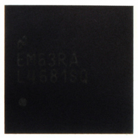
LM4681SQ/NOPB National Semiconductor, LM4681SQ/NOPB Datasheet

LM4681SQ/NOPB
Specifications of LM4681SQ/NOPB
LM4681SQTR
Related parts for LM4681SQ/NOPB
LM4681SQ/NOPB Summary of contents
Page 1
... The LM4681 is available in a 48-lead LLP package, ideal for portable and desktop computer applications. Block Diagram BOOMER ™ trademark of National Semiconductor Corporation. © 2006 National Semiconductor Corporation 2 C/SPI Volume Control Key Specifications n P ...
Page 2
Connection Diagram www.national.com LLP Package Top View Order Number LM4681SQ See NS Package Number SQA048AA (LLP Package) 2 20118917 ...
Page 3
3 www.national.com ...
Page 4
... Absolute Maximum Ratings If Military/Aerospace specified devices are required, please contact the National Semiconductor Sales Office/ Distributors for availability and specifications. Supply Voltage Input Voltage Power Dissipation (Note 3) ESD Susceptibility(Note 4) ESD Susceptibility (Note 5) Junction Temperature (Note 6) Storage Temperature Soldering Information Electrical Characteristics The following specifications apply for V wise specified ...
Page 5
Electrical Characteristics The following specifications apply for V wise specified. Limits apply for T = 25˚C. A Symbol Parameter PSRR Power Supply Rejection Ratio Headphone Amplifiers Maximum Power Output Per P O Channel THD+N Distortion + Noise V Output Noise ...
Page 6
I C/SPI Interface Controls Address Mode Control Register Volume Control Register (See Table 4 ) Headphone Control HP Sense Pin (HPSEL, pin 22) 0 ...
Page 7
Typical Performance Characteristics (Volume control at maximum, unless otherwise stated.) Class D Amplifier THD+N vs Frequency 8Ω Class D Amplifier THD+N vs Frequency V = 15.5V 8Ω ...
Page 8
Typical Performance Characteristics Class D Amplifier THD+N vs Output Power 8Ω Both channel driven, both measured Class D Amplifier THD+N vs Output Power V = 15.5V Both channel driven, both ...
Page 9
Typical Performance Characteristics Class D Amplifier Output Power vs Supply Voltage Class D Amplifier Magnitude vs Frequency 8Ω Class D Amplifier Magnitude vs Frequency V = 15.5V 8Ω, P ...
Page 10
Typical Performance Characteristics Class AB Headphone Amplifier Magnitude vs Frequency V = 12V 32Ω PSRR vs Frequency PSRR vs Frequency V = 15.5V DD www.national.com (Continued) Class AB Headphone Amplifier Magnitude ...
Page 11
Typical Performance Characteristics Class D Amplifier Dissipation vs Load Dissipation V = 12V 8Ω Both channels driven and measured Class D Amplifier Efficiency vs Total Output Power 8Ω Both ...
Page 12
Typical Performance Characteristics Output Power vs Load Resistance V = 12V, DD Upper curve = 10% THD+N, Lower curve = 1% THD+N Power Supply Current vs Power Supply Voltage www.national.com (Continued) Output Power vs Load Resistance Upper curve = 10% ...
Page 13
General Features SYSTEM FUNCTIONAL INFORMATION Modulation Technique Unlike typical Class D amplifiers that use single-ended com- parators to generate a pulse-width modulated switching waveform and RC timing circuits to set the switching fre- quency, the LM4681 uses a balanced differential ...
Page 14
General Features (Continued) Thermal Protection The LM4681 has thermal shutdown circuitry that monitors the die temperature. Once the LM4681 die temperature reaches 170˚C, the LM4681 disables the output switching waveform and remains disabled until the die temperature falls below 140˚C ...
Page 15
General Features (Continued Timing Diagrams SPI Timing Diagram SPI Operational Requirements 1. The maximum clock rate is 5MHz for the CLK pin. 2. CLK must remain logic-high for at least 100ns (t the rising edge of CLK, ...
Page 16
General Features (Continued ENABLE is logic-low for more than 8 CLK pulses then only the first 8 data bits will be latched and activated at rising edge of eighth CLK. 9. ENABLE must remain logic-high for at least ...
Page 17
Application Hints SUPPLY BYPASSING Correct power supply bypassing has two important goals. The first is to reduce noise on the power supply lines and minimize deleterious effects that the noise may cause to the amplifier’s operation. The second is to ...
Page 18
Revision History Rev 1.0 1.1 1.2 1.3 www.national.com Date 2/09/06 2/10/06 Edited the PSRR Typical values in the Elect. Char table. 3/08/06 Did few texts (Gen Desc section) clean-up, then re-released 3/17/06 Changed the typo under PSRR (Conditions-Vripple from 20mVp-p ...
Page 19
... BANNED SUBSTANCE COMPLIANCE National Semiconductor manufactures products and uses packing materials that meet the provisions of the Customer Products Stewardship Specification (CSP-9-111C2) and the Banned Substances and Materials of Interest Specification (CSP-9-111S2) and contain no ‘‘Banned Substances’’ as defined in CSP-9-111S2. ...


