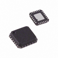
ADL5310ACP-R2 Analog Devices Inc, ADL5310ACP-R2 Datasheet

ADL5310ACP-R2
Specifications of ADL5310ACP-R2
Related parts for ADL5310ACP-R2
ADL5310ACP-R2 Summary of contents
Page 1
FEATURES 2 independent channels optimized for photodiode interfacing 6-decade input dynamic range Law conformance 0.3 dB from Temperature-stable logarithmic outputs Nominal slope 10 mV/dB (200 mV/dec), externally scalable Intercepts may be independently set by external ...
Page 2
ADL5310 TABLE OF CONTENTS Specifications..................................................................................... 3 Absolute Maximum Ratings............................................................ 4 Pin Configuration and Function Descriptions............................. 5 Typical Performance Characteristics ............................................. 6 General Structure............................................................................ 11 Theory.......................................................................................... 11 Managing Intercept and Slope .................................................. 12 Response Time and Noise Considerations.............................. 12 REVISION HISTORY ...
Page 3
SPECIFICATIONS 25° 665 kΩ, and VRDZ connected to VREF, unless otherwise noted. A REF Table 1. Parameter INPUT INTERFACE Specified Current Range Input Current Min/Max Limits ...
Page 4
ADL5310 ABSOLUTE MAXIMUM RATINGS Table 2. Parameter Supply Voltage V − Input Current Internal Power Dissipation θ JA Maximum Junction Temperature Operating Temperature Range Storage Temperature Range Lead Temperature Range (Soldering 60 sec) 1 With paddle soldered ...
Page 5
PIN CONFIGURATION AND FUNCTION DESCRIPTIONS Table 3. Pin Function Descriptions Pin No. Mnemonic Function 1, 6 VSUM Guard Pin. Used to shield the INP1 and INP2 input current lines, and for optional adjustment of the input summing node potentials. Pin ...
Page 6
ADL5310 TYPICAL PERFORMANCE CHARACTERISTICS 665 kΩ 25°C, unless otherwise noted. REF 1 –40°C, 0°C, +25°C, +70°C, +85° 1.4 1.2 1.0 0.8 ...
Page 7
I (A) REF Figure 9. V vs. I for Multiple Values of I LOG REF Decade Steps from 3 ...
Page 8
ADL5310 15 30nA 10 300nA 5 3nA 0 –5 –10 –15 –20 –25 –30 –35 –40 –45 –50 100 1k 10k 100k 1M FREQUENCY (Hz) Figure 15. Small Signal AC Response, I (5% Sine Modulation, Decade Steps from 3 nA ...
Page 9
MEAN + 3σ –5 MEAN – 3σ –10 –15 –20 –25 –40 –30 –20 – TEMPERATURE (°C) Figure 21. V Drift vs. Temperature (3σ to Either Side of ...
Page 10
ADL5310 700 600 500 400 300 200 100 0 190 195 200 SLOPE (mV/dec) Figure 27. Distribution of Logarithmic Slope 600 500 400 300 200 100 0 100 200 300 INTERCEPT (pA) Figure 28. Distribution of Logarithmic Intercept 700 600 ...
Page 11
GENERAL STRUCTURE The ADL5310 addresses a wide variety of interfacing conditions to meet the needs of fiber optic supervisory systems and is useful in many nonoptical applications. These notes explain the structure of this unique style of translinear log amp. ...
Page 12
ADL5310 The voltage V is generated by applying I LOG resistance of 4.55 kΩ, formed by the parallel combination of a 6.69 kΩ resistor to ground and a 14.2 kΩ resistor to Pin VRDZ (typically tied to the 2.5 V ...
Page 13
APPLICATIONS I RF1 2kΩ 4.7nF V BIAS I PD1 1kΩ 1nF 2kΩ 4.7nF V BIAS I RF2 I PD2 1kΩ 1nF 1nF The ADL5310 is easy to use in optical supervisory systems and in similar situations where a wide-ranging current ...
Page 14
ADL5310 The optional capacitor from LOG1 (LOG2) to ground forms a single-pole, low-pass filter in combination with the 5 kΩ resis- tance at this pin. For example, when using corner frequency is 3.2 kHz. Such filtering ...
Page 15
capacitor on each VSUM pin (20 nF parallel equivalent) combined with the 16 kΩ source resistance yields a 500 Hz pole, which is sufficiently below the bandwidth for the minimum input current of 3 nA. Residual crosstalk ...
Page 16
ADL5310 The solution in Figure longer subject to potential channel mismatch issues. Individual channel slope and intercept characteristics can be calibrated independently. The accuracy was verified using a pair of calibrated current sources. The performance of the ...
Page 17
EVALUATION BOARD An evaluation board is available for the ADL5310 (Figure 40 shows the schematic). It can be configured for a wide variety of experiments. The gain of each buffer amp is factory-set to unity, providing a slope of 200 ...
Page 18
ADL5310 PHOTODIODE C1 0.01µF R1 VSUM OPEN INP1 IRF1 IRF2 INP2 R15 R14 R13 R12 1kΩ 2kΩ 2kΩ 1kΩ C13 C12 C11 C10 1nF 4.7nF 4.7nF 1nF PHOTODIODE C7 0.01µF VRDZ VNEG ...
Page 19
Figure 41. Component-Side Layout Figure 42. Component-Side Silkscreen Rev Page ADL5310 ...
Page 20
... INDICATOR 1.00 0.85 0.80 SEATING PLANE ORDERING GUIDE Model Temperature Range ADL5310ACP-R2 –40°C to +85°C ADL5310ACP-REEL7 –40°C to +85°C ADL5310-EVAL 1 Branding is as follows: Line 1 — JQA Line 2 — Lot Code Line 3 — (Date Code) Date Code is in YYWW format © ...


