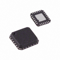
ADL5310ACP-R2 Analog Devices Inc, ADL5310ACP-R2 Datasheet - Page 17

ADL5310ACP-R2
Manufacturer Part Number
ADL5310ACP-R2
Description
IC LOGARITHMIC CONV DUAL 24LFCSP
Manufacturer
Analog Devices Inc
Type
Logarithmic Converterr
Datasheet
1.ADL5310ACPZ-REEL7.pdf
(20 pages)
Specifications of ADL5310ACP-R2
Design Resources
Interfacing ADL5315 to Translinear Logarithmic Amplifier (CN0056) Interfacing ADL5317 High Side Current Mirror to a Translinear Logarithmic Amplifier in an Avalanche Photodiode Power Detector
Applications
Fiber Optics
Mounting Type
Surface Mount
Package / Case
24-LFCSP
Lead Free Status / RoHS Status
Contains lead / RoHS non-compliant
Other names
ADL5310ACP-R2CT
EVALUATION BOARD
An evaluation board is available for the ADL5310 (Figure 40 shows the schematic). It can be configured for a wide variety of experiments.
The gain of each buffer amp is factory-set to unity, providing a slope of 200 mV/dec, and the intercept is set to 300 pA. Table 4 describes
the various configuration options.
Table 4. Evaluation Board Configuration Options
Component
P1
P2, R1, R3, R8, R9,
R17, R22, R25, R30
R5, R6, R7, R16,
R18, R19, R20,
R21, R31, R32, C4,
C14, C15, C16,
C19, C20
R2, R28, R29
R4, R10, R11, C2,
C3, C5, C6, C8, C9
C1, C7
R12, R13, R14,
R15, C10, C11,
C12, C13
IREF, INPT
J1, J2
Function
Supply Interface. Provides access to the Supply Pins VNEG, COMM, and
VPOS.
Monitor Interface. By adding 0 Ω resistors to R1, R3, R8, R9, R17, R22, and
R25, the VRDZ, VREF, VSUM, BIN1, BIN2, OUT1, and OUT2 pin voltages
can be monitored using a high impedance probe. VBIAS allows for the
external bias voltages to be applied to J1 and J2. If R30 = 0 Ω,
VBIAS = VREF.
Buffer Amplifier/Output Interface. The logarithmic slopes of the ADL5310
can be altered using each buffer’s gain-setting resistors, R5 and R6, and
R18 and R19. R7, R16, R31, R32, C19, and C20 allow for variation in the
buffer loading. R20, R21, C4, C14, C15, and C16 are provided for a variety
of filtering applications.
Intercept Adjustment. The voltage dropped across Resistors R28 and R29
determines the intercept reference current for each log amp, nominally
set to 3 µA using a 665 kΩ 1% resistor. R2 can be used to adjust the
output offset voltage at the LOG1 and LOG2 outputs.
Supply Decoupling.
Filtering VSUM.
Input Compensation. Provides essential HF compensation at the Input
Pins INP1, INP2, IRF1, and IRF2.
Input Interface. The test board is configured to accept current through the
SMA connectors labeled INP1 and INP2. Through-holes are provided to
connect photodiodes in place of the INP1 and INP2 SMAs for optical
interfacing. By removing R28 (R29 for INP2), a second current can be
applied to the IRF1 (IRF2 for INP2) input (also SMA) for evaluating the
ADL5310 in log ratio applications.
photodiodes.
SC-Style Photodiode. Provides for the direct mounting of SC-style
Rev. A | Page 17 of 20
Default Condition
P1 = installed
P2 = not installed
R1 = R3 = R8 = open (size 0402)
R9 = R17 = open (size 0402)
R22 = R25 = R30 = open (size 0402)
R5 = R19 = 0 Ω (size 0402)
R7 = R16 = 0 Ω (size 0402)
R20 = R21 = 0 Ω (size 0402)
R6 = R18 = open (size 0402)
R31 = R32 = open (size 0402)
C4 = C14 = open (size 0402)
C19 = C20 = open (size 0402)
C15 = C16 = open (size 0402)
LOG1 = OUT1 = installed
LOG2 = OUT2 = installed
R28 = R29 = 665 kΩ (size 0402)
R2 = 0 Ω (size 0402)
C2 = C5 = C9 = 100 pF (size 0402)
C3 = C6 = C8 = 0.01 µF (size 0402)
R4 = R10 = R11 = 0 Ω (size 0402)
C1 = C7 = 0.01 µF (size 0402)
R12 = R15 = 1 kΩ (size 0402)
R13 = R14 = 2 kΩ (size 0402)
C10 = C13 = 1 nF (size 0402)
C11 = C12 = 4.7 nF (size 0402)
IREF = INPT = installed
J1 = J2 = open
ADL5310


