AD534JH Analog Devices Inc, AD534JH Datasheet - Page 12
AD534JH
Manufacturer Part Number
AD534JH
Description
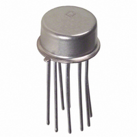
IC MULT DIV LASER TRIM TO100-10
Manufacturer
Analog Devices Inc
Specifications of AD534JH
Rohs Status
RoHS non-compliant
Function
Analog Multiplier/Divider
Number Of Bits/stages
4-Quadrant
Package / Case
TO-100, Metal Can (10 Leads)
No. Of Multipliers / Dividers
1
No. Of Amplifiers
1
Supply Voltage Range
± 8V To ± 18V
Slew Rate
20V/µs
Operating Temperature Range
0°C To +70°C
Digital Ic Case Style
TO-100
No. Of Pins
10
Lead Free Status / RoHS Status
Contains lead / RoHS non-compliant
Available stocks
Company
Part Number
Manufacturer
Quantity
Price

Part Number:
AD534JH
Manufacturer:
ADI/亚德诺
Quantity:
20 000


FUNCTIONAL DESCRIPTION
Figure 1 shows a functional block diagram of the AD534. Inputs
are converted to differential currents by three identical voltage-
to-current converters, each trimmed for zero offset. The product
of the X and Y currents is generated by a multiplier cell using
Gilbert’s translinear technique. An on-chip buried Zener
provides a highly stable reference, which is laser trimmed to
provide an overall scale factor of 10 V. The difference between
XY/SF and Z is then applied to the high gain output amplifier.
This permits various closed-loop configurations and dramati-
cally reduces nonlinearities due to the input amplifiers, a
dominant source of distortion in earlier designs.
The effectiveness of the new scheme can be judged from the
fact that, under typical conditions as a multiplier, the nonlinear-
ity on the Y input, with X at full scale (±10 V), is ±0.005% of FS.
Even at its worst point, which occurs when X = ±6.4 V, nonlinear-
ity is typically only ±0.05% of FS. Nonlinearity for signals applied
to the X input, on the other hand, is determined almost entirely
by the multiplier element and is parabolic in form. This error is a
major factor in determining the overall accuracy of the unit and
therefore is closely related to the device grade.
The generalized transfer function for the AD534 is given by
where:
A is the open-loop gain of the output amplifier, typically
70 dB at dc.
X
peak = ±1.25 SF).
SF is the scale factor, pretrimmed to 10.00 V but adjustable by
the user down to 3 V.
In most cases, the open-loop gain can be regarded as infinite,
and SF is 10 V. The operation performed by the AD534, can
then be described in terms of the following equation:
The user can adjust SF for values between 10.00 V and 3 V by
connecting an external resistor in series with a potentiometer
between SF and −V
resistance for a given value of SF is given by the relationship:
Due to device tolerances, allowance should be made to vary R
by ±25% using the potentiometer. Considerable reduction in
bias currents, noise, and drift can be achieved by decreasing SF.
This has the overall effect of increasing signal gain without the
customary increase in noise. Note that the peak input signal is
always limited to 1.25 SF (that is, ±5 V for SF = 4 V) so the
overall transfer function shows a maximum gain of 1.25. The
performance with small input signals, however, is improved by
using a lower scale factor because the dynamic range of the
AD534
1
, Y
(X
1
V
R
, Z
OUT
S
1
F
1
− X
, X
=
=
2
5
2
, Y
)(Y
4 .
A
kΩ
2
(
, and Z
1
X
−Y
1
0 1
−
S
. The approximate value of the total
2
SF
X
−
) = 10 V (Z
2
SF
2
SF
are the input voltages (full scale = ±SF,
)(
Y
1
−
Y
2
) (
1
− Z
−
Z
2
1
)
−
Z
2
)
Rev. C | Page 12 of 20
SF
inputs is now fully utilized. Bandwidth is unaffected by the use
of this option.
Supply voltages of ±15 V are generally assumed. However,
satisfactory operation is possible down to ±8 V (see Figure 7).
Because all inputs maintain a constant peak input capability of
±1.25 SF, some feedback attenuation is necessary to achieve
output voltage swings in excess of ±12 V when using higher
supply voltages.
PROVIDES GAIN WITH LOW NOISE
The AD534 is the first general-purpose multiplier capable of
providing gains up to ×100, frequently eliminating the need for
separate instrumentation amplifiers to precondition the inputs.
The AD534 can be very effectively employed as a variable gain
differential input amplifier with high common-mode rejection.
The gain option is available in all modes and simplifies the
implementation of many function-fitting algorithms such as
those used to generate sine and tangent. The utility of this
feature is enhanced by the inherent low noise of the AD534:
90 μV rms (depending on the gain), a factor of 10 lower than
previous monolithic multipliers. Drift and feedthrough are also
substantially reduced over earlier designs.
OPERATION AS A MULTIPLIER
Figure 15 shows the basic connection for multiplication. Note
that the circuit meets all specifications without trimming.
To reduce ac feedthrough to a minimum (as in a suppressed
carrier modulator), apply an external trim voltage (±30 mV
range required) to the X or Y input (see Figure 3). Figure 10
shows the typical ac feedthrough with this adjustment mode.
Note that the Y input is a factor of 10 lower than the X input
and should be used in applications where null suppression is
critical.
The high impedance Z
sum an additional signal into the output. In this mode, the
output amplifier behaves as a voltage follower with a 1 MHz
small signal bandwidth and a 20 V/μs slew rate. This terminal
should always be referenced to the ground point of the driven
system, particularly if this is remote. Likewise, the differential
inputs should be referenced to their respective ground poten-
tials to realize the full accuracy of the AD534.
A much lower scaling voltage can be achieved without any
reduction of input signal range using a feedback attenuator as
shown in Figure 16. In this example, the scale is such that V
X INPUT
±12V PK
Y INPUT
±12V PK
±10V FS
±10V FS
Figure 15. Basic Multiplier Connection
X
X
SF
Y
Y
1
2
1
2
AD534
2
terminal of the AD534 can be used to
OUT
+V
–V
Z
Z
S
S
1
2
+15V
–15V
OUTPUT, ±12V PK =
OPTIONAL SUMMING
INPUT, Z, ±10V PK
(X1 – X
2
10V
) (Y1 – Y
2
)
+ Z
2
OUT
=
Related parts for AD534JH
Image
Part Number
Description
Manufacturer
Datasheet
Request
R

Part Number:
Description:
±1.7g Dual-Axis IMEMS Accelerometer Evaluation Board
Manufacturer:
Analog Devices Inc
Datasheet:

Part Number:
Description:
Inertial Sensor Evaluation System
Manufacturer:
Analog Devices Inc
Datasheet:
Part Number:
Description:
Manufacturer:
Analog Devices Inc
Datasheet:
Part Number:
Description:
Manufacturer:
Analog Devices Inc
Datasheet:
Part Number:
Description:
Manufacturer:
Analog Devices Inc
Datasheet:
Part Number:
Description:
Manufacturer:
Analog Devices Inc
Datasheet:
Part Number:
Description:
Manufacturer:
Analog Devices Inc
Datasheet:
Part Number:
Description:
Manufacturer:
Analog Devices Inc
Datasheet:
Part Number:
Description:
Manufacturer:
Analog Devices Inc
Datasheet:
Part Number:
Description:
Manufacturer:
Analog Devices Inc
Datasheet:
Part Number:
Description:
Manufacturer:
Analog Devices Inc
Datasheet:
Part Number:
Description:
Manufacturer:
Analog Devices Inc
Datasheet:
Part Number:
Description:
Manufacturer:
Analog Devices Inc
Datasheet: