AD534JH Analog Devices Inc, AD534JH Datasheet - Page 7
AD534JH
Manufacturer Part Number
AD534JH
Description
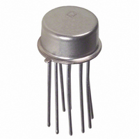
IC MULT DIV LASER TRIM TO100-10
Manufacturer
Analog Devices Inc
Specifications of AD534JH
Rohs Status
RoHS non-compliant
Function
Analog Multiplier/Divider
Number Of Bits/stages
4-Quadrant
Package / Case
TO-100, Metal Can (10 Leads)
No. Of Multipliers / Dividers
1
No. Of Amplifiers
1
Supply Voltage Range
± 8V To ± 18V
Slew Rate
20V/µs
Operating Temperature Range
0°C To +70°C
Digital Ic Case Style
TO-100
No. Of Pins
10
Lead Free Status / RoHS Status
Contains lead / RoHS non-compliant
Available stocks
Company
Part Number
Manufacturer
Quantity
Price

Part Number:
AD534JH
Manufacturer:
ADI/亚德诺
Quantity:
20 000


ABSOLUTE MAXIMUM RATINGS
Table 3.
Parameter
Supply Voltage
Internal Power Dissipation
Output Short Circuit to
Input Voltages (X
Rated Operating
Storage Temperature
Lead Temperature Range,
Stresses above those listed under Absolute Maximum Ratings
may cause permanent damage to the device. This is a stress
rating only; functional operation of the device at these or any
other conditions above those indicated in the operational
section of this specification is not implied. Exposure to absolute
maximum rating conditions for extended periods may affect
device reliability.
THERMAL RESISTANCE
θ
soldered in a circuit board for surface-mount packages.
Table 4. Thermal Resistance
Package Type
10-Pin TO-100 (H-10)
14-Lead SBDIP (D-14)
20-Terminal LCC (E-20-1)
JA
Ground
Z
Temperature Range
Range
60 sec Soldering
is specified for the worst-case conditions, that is, a device
1
, Z
2
)
1
, X
2
, Y
1
, Y
2
,
AD534J,
AD534K,
AD534L
±18 V
500 mW
Indefinite
±V
0°C to +70°C
−65°C to +150°C
300°C
S
θ
150
95
95
JA
θ
25
25
25
JC
AD534S,
AD534T
±22 V
500 mW
Indefinite
±V
−55°C to +125°C
−65°C to +150°C
300°C
S
Unit
°C/W
°C/W
°C/W
Rev. C | Page 7 of 20
Contact factory for latest dimensions.
ESD CAUTION
SF
X
Y
2
1
X
Figure 2. Chip Dimensions and Bonding Diagram
1
Y
50kΩ
2
Figure 3. Optional Trimming Configuration
Dimensions shown in inches and (mm)
+V
–V
S
S
470kΩ
0.100 (2.54)
+V
1kΩ
S
–V
S
A
5
3
4
8
TO APPROPRIATE
INPUT TERMINAL
OUT
Z
2
AD534
Z
(1.93)
0.076
1
Related parts for AD534JH
Image
Part Number
Description
Manufacturer
Datasheet
Request
R

Part Number:
Description:
±1.7g Dual-Axis IMEMS Accelerometer Evaluation Board
Manufacturer:
Analog Devices Inc
Datasheet:

Part Number:
Description:
Inertial Sensor Evaluation System
Manufacturer:
Analog Devices Inc
Datasheet:
Part Number:
Description:
Manufacturer:
Analog Devices Inc
Datasheet:
Part Number:
Description:
Manufacturer:
Analog Devices Inc
Datasheet:
Part Number:
Description:
Manufacturer:
Analog Devices Inc
Datasheet:
Part Number:
Description:
Manufacturer:
Analog Devices Inc
Datasheet:
Part Number:
Description:
Manufacturer:
Analog Devices Inc
Datasheet:
Part Number:
Description:
Manufacturer:
Analog Devices Inc
Datasheet:
Part Number:
Description:
Manufacturer:
Analog Devices Inc
Datasheet:
Part Number:
Description:
Manufacturer:
Analog Devices Inc
Datasheet:
Part Number:
Description:
Manufacturer:
Analog Devices Inc
Datasheet:
Part Number:
Description:
Manufacturer:
Analog Devices Inc
Datasheet:
Part Number:
Description:
Manufacturer:
Analog Devices Inc
Datasheet: