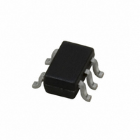
LMV331M7X/NOPB National Semiconductor, LMV331M7X/NOPB Datasheet - Page 10

LMV331M7X/NOPB
Manufacturer Part Number
LMV331M7X/NOPB
Description
IC COMP TINY LOW VOLT SC-70-5
Manufacturer
National Semiconductor
Type
General Purposer
Datasheet
1.LMV331M5XNOPB.pdf
(20 pages)
Specifications of LMV331M7X/NOPB
Number Of Elements
1
Output Type
CMOS, Open-Collector, TTL
Voltage - Supply
2.7 V ~ 5.5 V
Mounting Type
Surface Mount
Package / Case
6-TSSOP (5 lead), SC-88A, SOT-353
Comparator Type
General Purpose
No. Of Comparators
1
Response Time
200ns
Ic Output Type
CMOS, MOS, Open-Collector / Drain, TTL
Supply Current
60µA
Supply Voltage Range
2.7V To 5V
Rohs Compliant
Yes
Lead Free Status / RoHS Status
Lead free / RoHS Compliant
Other names
LMV331M7X
LMV331M7XTR
LMV331M7XTR
Available stocks
Company
Part Number
Manufacturer
Quantity
Price
www.national.com
PULSE GENERATOR WITH VARIABLE DUTY CYCLE
The pulse generator with variable duty cycle is just a minor
modification of the basic square wave generator. Providing a
separate charge and discharge path for capacitor C
ates a variable duty cycle. One path, through R
charge the capacitor and set the pulse width (t
path, R
between pulses (t
By varying resistor R
erator can be changed without changing the pulse width.
Similarly, by varying R
affecting the time between pulses. Both controls will change
the frequency of the generator. The pulse width and time be-
tween pulses can be found from:
1
and D
FIGURE 6. Crystal controlled Oscillator
1
FIGURE 7. Pulse Generator
will discharge the capacitor and set the time
2
).
1
2
, the time between pulses of the gen-
, the pulse width will be altered without
1
2
). The other
and D
10008009
10008007
1
gener-
2
will
10
Solving these equations for t
These terms will have a slight error due to the fact that V
is not exactly equal to 2/3 V
diode drop to:
POSITIVE PEAK DETECTOR
Positive peak detector is basically the comparator operated
as a unit gain follower with a large holding capacitor from the
output to ground. Additional transistor is added to the output
to provide a low impedance current source. When the output
of the comparator goes high, current is passed through the
transistor to charge up the capacitor. The only discharge path
will be the 1 MΩ resistor shunting C1 and any load that is
connected to the output. The decay time can be altered simply
by changing the 1 MΩ resistor. The output should be used
through a high impedance follower to a avoid loading the out-
put of the peak detector.
t
t
1
2
=R
=R
CC
1
4
5
and t
C
C
but is actually reduced by the
1
1
ln2
ln2
2
max


