LM319M/NOPB National Semiconductor, LM319M/NOPB Datasheet - Page 2
LM319M/NOPB
Manufacturer Part Number
LM319M/NOPB
Description
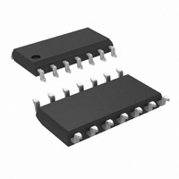
IC COMPARATOR DUAL HI SPD 14SOIC
Manufacturer
National Semiconductor
Type
General Purposer
Specifications of LM319M/NOPB
Number Of Elements
2
Output Type
DTL, Open-Collector, Open-Emitter, RTL, TTL
Voltage - Supply
5 V ~ 30 V, ±2.5 V ~ 15 V
Mounting Type
Surface Mount
Package / Case
14-SOIC (0.154", 3.90mm Width)
Amplifier Type
Comparator
Current, Input Bias
250 nA
Current, Input Offset
80 nA
Current, Supply
-3 to +8 mA
Number Of Amplifiers
Dual
Package Type
DIP-8
Power Dissipation
500 mW
Temperature, Operating, Range
0 to +70 °C
Voltage, Gain
40 V/mV
Voltage, Input
±15 V
Voltage, Input Offset
2 mV
Voltage, Supply
5 to 36 V
Comparator Type
High Speed
No. Of Comparators
2
Response Time
80ns
Ic Output Type
DTL, RTL, TTL
Supply Current
8mA
Supply Voltage Range
5V To 36V
Amplifier Case Style
SOIC
Rohs Compliant
Yes
Output Compatibility
DTL, RTL, TTL
Lead Free Status / RoHS Status
Lead free / RoHS Compliant
Other names
*LM319M
*LM319M/NOPB
LM319M
*LM319M/NOPB
LM319M
Available stocks
Company
Part Number
Manufacturer
Quantity
Price

Part Number:
LM319M/NOPB
Manufacturer:
NS
Quantity:
20 000


www.national.com
Input Offset Voltage (Note 6)
Input Bias Current
Voltage Gain
Response Time (Note 7)
Output Leakage Current
Input Offset Voltage (Note 6)
Differential Input Voltage
Input Offset Current (Note 6)
Saturation Voltage
Input Offset Current (Note 6)
Input Bias Current
Input Voltage Range
Saturation Voltage
Output Leakage Current
Positive Supply Current
Positive Supply Current
Negative Supply Current
Electrical Characteristics
Note 3: For supply voltages less than
Note 4: The maximum junction temperature of the LM119 is 150˚C, while that of the LM219 is 110˚C. For operating at elevated temperatures, devices in the H10
package must be derated based on a thermal resistance of 160˚C/W, junction to ambient, or 19˚C/W, junction to case. The thermal resistance of the J14 and N14
packages is 100˚C/W, junction to ambient.
Note 5: These specifications apply for V
temperature specifications are limited to −25˚C
single 5V supply up to
Note 6: The offset voltages and offset currents given are the maximum values required to drive the output within a volt of either supply with a 1 mA load. Thus, these
parameters define an error band and take into account the worst case effects of voltage gain and input impedance.
Note 7: The response time specified (see definitions) is for a 100 mV input step with 5 mV overdrive.
Note 8: Output is pulled up to 15V through a 1.4 k
Note 9: Refer to RETS119X for LM119H/883 and LM119J/883 specifications.
Absolute Maximum Ratings
If Military/Aerospace specified devices are required,
please contact the National Semiconductor Sales Office/
Distributors for availability and specifications.
Total Supply Voltage
Output to Negative Supply Voltage
Ground to Negative Supply Voltage
Ground to Positive Supply Voltage
Differential Input Voltage
Input Voltage (Note 3)
ESD rating (1.5 k
Power Dissipation (Note 4)
Output Short Circuit Duration
Storage Temperature Range
100 pF)
Parameter
±
15V supplies. Do not operate the device with more than 16V from ground to V
in series with
±
S
15V the absolute maximum input voltage is equal to the supply voltage.
=
±
15V, and the Ground pin at ground, and −55˚C
T
T
T
T
T
T
V
T
V
T
R
V
V
V
V
T
T
V
V
T
T
T
A
A
A
A
A
A
A
A
A
A
A
A
A
IN
IN
S
+
+
IN
IN
−
S
resistor.
= 25˚C, R
= 25˚C
= 25˚C
= 25˚C (Note 8)
= 25˚C, V
= 25˚C
= 25˚C
= 5V, V
= V
= 25˚C, V
= 25˚C, V
= 25˚C, V
=
+85˚C. The offset voltage, offset current and bias current specifications apply for any supply voltage from a
(Note 5)
4.5V, V
0˚C
0˚C
5k
±
−65˚C to 150˚C
−5 mV, I
5 mV, V
−6 mV, I
5 mV, V
GND
15V
(Note 9)
−
= 0V
Conditions
−
500 mW
= 0
S
S
+
S
S
OUT
OUT
OUT
= 0
SINK
10 sec
= 5V, V
=
=
=
±
800V
±
5k
36V
36V
25V
18V
15V
±
±
±
5V
= 35V
= 35V,
15V
15V
15V
= 25 mA
3.2 mA
−
2
= 0
Lead Temperature
Soldering Information
Operating Temperature Range
See AN-450 “Surface Mounting Methods and Their Effect
on Product Reliability” for other methods of soldering
surface mount devices.
(Soldering, 10 sec.)
Dual-In-Line Package
Small Outline Package
LM119
LM219
Soldering (10 seconds)
Vapor Phase (60 seconds)
Infrared (15 seconds)
T
A
+125˚C, unless otherwise stated. With the LM219, however, all
Min
−12
S
10
1
.
LM119/LM219
0.75
0.23
Typ
±
150
0.7
0.2
4.3
30
40
80
1
8
3
13
1000
Max
11.5
500
100
+12
4.0
1.5
0.4
0.6
4.5
75
10
±
2
7
3
5
−55˚C to 125˚C
−25˚C to 85˚C
Units
V/mV
mV
mV
mA
mA
mA
260˚C
260˚C
215˚C
220˚C
nA
nA
µA
nA
nA
µA
ns
V
V
V
V
V
V
Related parts for LM319M/NOPB
Image
Part Number
Description
Manufacturer
Datasheet
Request
R

Part Number:
Description:
SENSOR 1PSIG 1/2NPT .5-4.5V 12"
Manufacturer:
Measurement Specialties Inc.
Datasheet:

Part Number:
Description:
SENSOR 5PSIG 1/2NPT .5-4.5V 12"
Manufacturer:
Measurement Specialties Inc.
Datasheet:

Part Number:
Description:
SENSOR 30PSIG 1/2NPT .5-4.5V 12"
Manufacturer:
Measurement Specialties Inc.
Datasheet:

Part Number:
Description:
National Semiconductor [8-Bit D/A Converter]
Manufacturer:
National Semiconductor
Datasheet:
Part Number:
Description:
National Semiconductor [Media Coprocessor]
Manufacturer:
National Semiconductor
Datasheet:
Part Number:
Description:
Digitally Controlled Tone and Volume Circuit with Stereo Audio Power Amplifier, Microphone Preamp Stage and National 3D Sound
Manufacturer:
National Semiconductor
Datasheet:
Part Number:
Description:
Digitally Controlled Tone and Volume Circuit with Stereo Audio Power Amplifier, Microphone Preamp Stage and National 3D Sound
Manufacturer:
National Semiconductor
Datasheet:
Part Number:
Description:
AC97 Rev 2 Codec with Sample Rate Conversion and National 3D Sound
Manufacturer:
National Semiconductor
Part Number:
Description:
Manufacturer:
National Semiconductor
Datasheet:
Part Number:
Description:
Manufacturer:
National Semiconductor
Datasheet:
Part Number:
Description:
General Purpose, Low Voltage, Low Power, Rail-to-Rail Output Operational Amplifiers
Manufacturer:
National Semiconductor
Datasheet:
Part Number:
Description:
8-bit 20 MSPS flash A/D converter.
Manufacturer:
National Semiconductor
Datasheet:
Part Number:
Description:
Low Noise Quad Operational Amplifier
Manufacturer:
National Semiconductor
Datasheet:
Part Number:
Description:
Quad Differential Line Receivers
Manufacturer:
National Semiconductor
Datasheet: