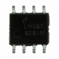
LMC6762BIM/NOPB National Semiconductor, LMC6762BIM/NOPB Datasheet - Page 4

LMC6762BIM/NOPB
Manufacturer Part Number
LMC6762BIM/NOPB
Description
IC COMP DUAL MICRPWR CMOS 8-SOIC
Manufacturer
National Semiconductor
Type
General Purposer
Datasheet
1.LMC6762AIMNOPB.pdf
(14 pages)
Specifications of LMC6762BIM/NOPB
Number Of Elements
2
Output Type
Push-Pull, Rail-to-Rail
Voltage - Supply
2.7 V ~ 15 V, ±1.35 V ~ 7.5 V
Mounting Type
Surface Mount
Package / Case
8-SOIC (0.154", 3.90mm Width)
Comparator Type
Micropower
No. Of Comparators
2
Response Time
4µs
Ic Output Type
Push Pull
Supply Current
25µA
Supply Voltage Range
2.7V To 15V
Amplifier Case Style
SOIC
No. Of Pins
8
Rohs Compliant
Yes
Dc
1012
Lead Free Status / RoHS Status
Lead free / RoHS Compliant
Other names
*LMC6762BIM
*LMC6762BIM/NOPB
LMC6762BIM
*LMC6762BIM/NOPB
LMC6762BIM
Available stocks
Company
Part Number
Manufacturer
Quantity
Price
Company:
Part Number:
LMC6762BIM/NOPB
Manufacturer:
TI
Quantity:
10 000
www.national.com
t
t
t
t
RISE
FALL
PHL
PLH
Symbol
AC Electrical Characteristics
Unless otherwise specified, all limits guaranteed for T
the temperature extreme.
Note 1: Absolute Maximum Ratings indicate limits beyond which damage to the device may occur. Operating Ratings indicate conditions for which the device is
intended to be functional, but specific performance is not guaranteed. For guaranteed specifications and the test conditions, see the electrical characteristics.
Note 2: Human body model, 1.5 kΩ in series with 100 pF.
Note 3: Applies to both single-supply and split-supply operation. Continuous short circuit operation at elevated ambient temperature can result in exceeding the
maximum allowed junction temperature of 150˚C. Output currents in excess of
Note 4: The maximum power dissipation is a function of T
P
Note 5: Typical Values represent the most likely parametric norm.
Note 6: All limits are guaranteed by testing or statistical analysis.
Note 7: Do not short circuit output to V
Note 8: Input Offset Voltage Average Drift is calculated by dividing the accelerated operating life drift average by the equivalent operational time. The Input Offset
Voltage Average Drift represents the input offset voltage change at worst-case input conditions.
Note 9: C
Note 10: The rise and fall times are measured with a 2V input step. The propagation delays are also measured with a 2V input step.
D
= (T
J(max)
L
Rise Time
Fall Time
Propagation Delay
(High to Low)
Propagation Delay
(Low to High)
includes the probe and jig capacitance.
– T
A
Parameter
)/θ
JA
.All numbers apply for packages soldered directly into a PC board.
+
f = 10 kHz, C
Overdrive = 10 mV (Notes 9, 10)
f = 10 kHz, C
Overdrive = 10 mV (Notes 9, 10)
f = 10 kHz,
C
(Notes 9, 10)
V
f = 10 kHz,
C
(Notes 9, 10)
f = 10 kHz,
C
(Notes 9, 10)
V
f = 10 kHz,
C
(Notes 9, 10)
, when V
+
+
L
L
L
L
= 50 pF
= 2.7V,
= 50 pF
= 50 pF
= 2.7V,
= 50 pF
+
is greater than 12V or reliability will be adversely affected.
L
L
= 50 pF,
= 50 pF,
Conditions
J(max)
, θ
Overdrive = 10 mV
Overdrive = 100 mV
Overdrive = 10 mV
Overdrive = 100 mV
Overdrive = 10 mV
Overdrive = 100 mV
Overdrive = 10 mV
Overdrive = 100 mV
J
= 25˚C, V
JA
, and T
±
4
30 mA over long term may adversely affect reliability.
A
. The maximum allowable power dissipation at any ambient temperature is
+
= 5V, V
−
= 0V, V
(Note 5)
Typ
0.3
0.3
10
10
4
4
6
4
7
4
CM
= V
O
LMC6762AI
= V
(Note 6)
Limit
+
/2. Boldface limits apply at
LMC6762BI
(Note 6)
Limit
Units
µs
µs
µs
µs
µs
µs
µs
µs
µs
µs


