AP6950GYT-HF Advanced Power Electronics Corp., AP6950GYT-HF Datasheet
AP6950GYT-HF
Specifications of AP6950GYT-HF


Related parts for AP6950GYT-HF

AP6950GYT-HF Summary of contents
Page 1
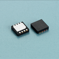
... Maximum Thermal Resistance, Junction-ambient Rthj-a Maximum Thermal Resistance, Junction-ambient Data & specifications subject to change without notice Dual N-CHANNEL ENHANCEMENT MODE POWER MOSFET D1 G1 D2/ S1/ Parameter 3 4 AP6950GYT-HF Halogen-Free Product CH-1 BV DSS R 18mΩ DS(ON CH-2 BV DSS R 10.5mΩ DS(ON ...
Page 2
... AP6950GYT-HF CH-1 Electrical Characteristics@T Symbol Parameter BV Drain-Source Breakdown Voltage DSS R Static Drain-Source On-Resistance DS(ON) V Gate Threshold Voltage GS(th) g Forward Transconductance fs I Drain-Source Leakage Current DSS I Gate-Source Leakage GSS Q Total Gate Charge g Q Gate-Source Charge gs Q Gate-Drain ("Miller") Charge gd t Turn-on Delay Time d(on) t Rise Time ...
Page 3
... GS I =11A D V =15V DS V =4. =15V =3.3Ω =10V =15V DS f=1.0MHz f=1.0MHz Test Conditions 2 I =11A =11A dI/dt=100A/µs AP6950GYT-HF Min. Typ 13 970 - 120 - 80 - 1.2 Min. Typ. ...
Page 4
... Fig 2. Typical Output Characteristics 2.0 = 1.6 1.2 0.8 0.4 - Fig 4. Normalized On-Resistance 2.0 1 0.8 0.4 0.0 1 1.2 1.4 -50 Fig 6. Gate Threshold Voltage v.s. AP6950GYT- =150 Drain-to-Source Voltage ( = =10V 100 Junction Temperature ( C) j v.s. Junction Temperature I =250uA ...
Page 5
... AP6950GYT-HF Channel = =15V Total Gate Charge (nC) G Fig 7. Gate Charge Characteristics 100 Operation in this area limited by R DS( Single Pulse 0.01 0.01 0 ,Drain-to-Source Voltage (V) DS Fig 9. Maximum Safe Operating Area 40 V =5V DS ...
Page 6
... Fig 2. Typical Output Characteristics 2.0 = 1.6 1.2 0.8 0.4 - Fig 4. Normalized On-Resistance 2.0 1 0.8 0.4 0.0 1 1.2 1.4 -50 Fig 6. Gate Threshold Voltage v.s. AP6950GYT- =150 Drain-to-Source Voltage ( =11A D V =10V 100 Junction Temperature ( C) j v.s. Junction Temperature I =250uA ...
Page 7
... AP6950GYT-HF Channel =11A D V =15V Total Gate Charge (nC) G Fig 7. Gate Charge Characteristics 100 Operation in this area limited by R DS( Single Pulse 0.01 0.01 0 ,Drain-to-Source Voltage (V) DS Fig 9. Maximum Safe Operating Area 60 V =5V ...