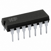
74HCT125N,652 NXP Semiconductors, 74HCT125N,652 Datasheet - Page 14

74HCT125N,652
Manufacturer Part Number
74HCT125N,652
Description
IC BUFFER DVR TRI-ST QD 14PDIP
Manufacturer
NXP Semiconductors
Series
74HCTr
Datasheets
1.74HCT4046ADB112.pdf
(19 pages)
2.74HCT4046ADB112.pdf
(23 pages)
3.74HCT125D653.pdf
(6 pages)
Specifications of 74HCT125N,652
Package / Case
14-DIP (0.300", 7.62mm)
Logic Type
Buffer/Line Driver, Non-Inverting
Number Of Elements
4
Number Of Bits Per Element
1
Current - Output High, Low
6mA, 6mA
Voltage - Supply
4.5 V ~ 5.5 V
Mounting Type
Through Hole
Logic Family
74HCT
Number Of Channels Per Chip
4
Polarity
Non-Inverting
Supply Voltage (max)
5.5 V
Supply Voltage (min)
4.5 V
Maximum Operating Temperature
+ 125 C
Mounting Style
Through Hole
High Level Output Current
- 6 mA
Input Bias Current (max)
8 uA
Low Level Output Current
6 mA
Minimum Operating Temperature
- 40 C
Output Type
3-State
Propagation Delay Time
12 ns
Number Of Lines (input / Output)
4 / 4
Lead Free Status / RoHS Status
Lead free / RoHS Compliant
Operating Temperature
-
Lead Free Status / Rohs Status
Lead free / RoHS Compliant
Other names
568-1510-5
74HCT125N
933757000652
74HCT125N
933757000652
Philips Semiconductors
AC waveforms 74HCT (continued)
Test circuit for 74HCT
March 1988
handbook, full pagewidth
handbook, full pagewidth
HCMOS family characteristics
Switch position
Note
1. For open-drain N-channel outputs t
TEST
t
t
t
t
C
R
PZH
PZL
PHZ
PLZ
L
T
=
=
load capacitance including jig and probe capacitance
(see AC CHARACTERISTICS for values).
termination resistance should be equal to the output impedance Z
the pulse generator.
SWITCH
GND
V
GND
V
CC
CC
LOW-to-OFF
OFF-to-LOW
HIGH-to-OFF
OFF-to-HIGH
MGK566
OUTPUT
OUTPUT
OUTPUT
ENABLE
GENERATOR
PULSE
Fig.11 Propagation delays of 3-state outputs.
90%
Fig.12 Test circuit for 3-state outputs.
PLZ
t f
1.3 V
10%
and t
V I
t PLZ
enabled
outputs
t PHZ
PZL
R T
are applicable.
10%
D.U.T
V CC
90%
14
o
of
disabled
outputs
V O
C L
t r
t PZL
t PZH
R L = 1 k
50 pF
FAMILY SPECIFICATIONS
1.3 V
MGK563
1.3 V
outputs
enabled
V CC


