NL27WZ126USG ON Semiconductor, NL27WZ126USG Datasheet - Page 5
NL27WZ126USG
Manufacturer Part Number
NL27WZ126USG
Description
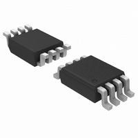
IC BUFFER DL TRI-ST NON-INV US8
Manufacturer
ON Semiconductor
Series
27WZr
Datasheet
1.NL27WZ126USG.pdf
(6 pages)
Specifications of NL27WZ126USG
Logic Type
Buffer/Line Driver, Non-Inverting
Number Of Elements
2
Number Of Bits Per Element
1
Current - Output High, Low
32mA, 32mA
Voltage - Supply
1.65 V ~ 5.5 V
Operating Temperature
-40°C ~ 85°C
Mounting Type
Surface Mount
Package / Case
US8, 8-VSSOP
Logic Family
LCX
Number Of Channels Per Chip
2
Polarity
Non-Inverting
Supply Voltage (max)
5.5 V
Supply Voltage (min)
1.65 V
Maximum Operating Temperature
+ 85 C
Mounting Style
SMD/SMT
High Level Output Current
- 32 mA
Low Level Output Current
32 mA
Maximum Power Dissipation
250 mW
Minimum Operating Temperature
- 40 C
Number Of Lines (input / Output)
2 / 3
Output Type
3-State
Propagation Delay Time
5.7 ns at 3.3 V, 5 ns at 5 V
Logic Device Type
Buffer, Non Inverting
Supply Voltage Range
1.65V To 5.5V
Logic Case Style
US8
No. Of Pins
8
Operating Temperature Range
-40°C To +85°C
Filter Terminals
SMD
Rohs Compliant
Yes
Family Type
27WZ
Lead Free Status / RoHS Status
Lead free / RoHS Compliant
Other names
NL27WZ126USGOS
NL27WZ126USGOS
NL27WZ126USGOSTR
NL27WZ126USGOS
NL27WZ126USGOSTR
Available stocks
Company
Part Number
Manufacturer
Quantity
Price

Part Number:
NL27WZ126USG
Manufacturer:
ON/安森美
Quantity:
20 000


†For information on tape and reel specifications, including part orientation and tape sizes, please refer to our Tape and Reel Packaging
DEVICE ORDERING INFORMATION
Specifications Brochure, BRD8011/D.
NL27WZ126US
NL27WZ126USG
Device Order
Number
A 1 MHz square input wave is recommended for
INPUT
Figure 6. t
propagation delay tests.
Indicator
Circuit
Logic
C
NL
NL
L
= 50 pF
PZL
Table 1. Output Enable and Disable Times
t
R
= t
2
Gates per
Symbol
Package
or t
No. of
F
V
V
= 2.5 ns, 10% to 90%; f = 1 MHz; t
mo
mi
2
2
V
PLZ
CC
R
R
1
L
= 500 W
= 500 W
Device Nomenclature
Identifier
OUTPUT
Range
Temp
3.3 V $ 0.3 V
7
7
1.5 V
1.5 V
http://onsemi.com
Technology
NL27WZ126
WZ
WZ
5
Function
2.7 V
1.5 V
1.5 V
V
Device
V
CC
126
126
CC
W
A 1 MHz square input wave is recommended for
= 500 nsv
INPUT
Package
Suffix
USG
US
2.5 V $ 0.2 V
Figure 7. t
propagation delay tests.
V
V
CC/
CC/
(Pb−Free)
2
2
Package
C
L
Type
US8
US8
= 50 pF
PZH
or t
PHZ
178 mm, 3000 Units
178 mm, 3000 Units
R
L
= 250 W
Reel Size
Tape and
OUTPUT
†
Related parts for NL27WZ126USG
Image
Part Number
Description
Manufacturer
Datasheet
Request
R

Part Number:
Description:
ON Semiconductor [VOLTAGE REGULATOR]
Manufacturer:
ON Semiconductor
Datasheet:
Part Number:
Description:
357-036-542-201 CARDEDGE 36POS DL .156 BLK LOPRO
Manufacturer:
ON Semiconductor
Datasheet:
Part Number:
Description:
357-036-542-201 CARDEDGE 36POS DL .156 BLK LOPRO
Manufacturer:
ON Semiconductor
Datasheet:
Part Number:
Description:
357-036-542-201 CARDEDGE 36POS DL .156 BLK LOPRO
Manufacturer:
ON Semiconductor
Datasheet:
Part Number:
Description:
357-036-542-201 CARDEDGE 36POS DL .156 BLK LOPRO
Manufacturer:
ON Semiconductor
Datasheet:
Part Number:
Description:
357-036-542-201 CARDEDGE 36POS DL .156 BLK LOPRO
Manufacturer:
ON Semiconductor
Datasheet:
Part Number:
Description:
357-036-542-201 CARDEDGE 36POS DL .156 BLK LOPRO
Manufacturer:
ON Semiconductor
Datasheet:
Part Number:
Description:
357-036-542-201 CARDEDGE 36POS DL .156 BLK LOPRO
Manufacturer:
ON Semiconductor
Datasheet:
Part Number:
Description:
357-036-542-201 CARDEDGE 36POS DL .156 BLK LOPRO
Manufacturer:
ON Semiconductor
Datasheet:
Part Number:
Description:
357-036-542-201 CARDEDGE 36POS DL .156 BLK LOPRO
Manufacturer:
ON Semiconductor
Datasheet:
Part Number:
Description:
357-036-542-201 CARDEDGE 36POS DL .156 BLK LOPRO
Manufacturer:
ON Semiconductor
Datasheet:
Part Number:
Description:
Manufacturer:
ON Semiconductor
Datasheet:
Part Number:
Description:
Manufacturer:
ON Semiconductor
Datasheet:
Part Number:
Description:
Manufacturer:
ON Semiconductor
Datasheet: