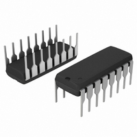
MC14526BCPG ON Semiconductor, MC14526BCPG Datasheet - Page 2

MC14526BCPG
Manufacturer Part Number
MC14526BCPG
Description
IC COUNTER BINARY 4BIT 16-DIP
Manufacturer
ON Semiconductor
Series
4000Br
Specifications of MC14526BCPG
Logic Type
Binary Counter, Decade
Direction
Down
Number Of Elements
1
Number Of Bits Per Element
4
Reset
Asynchronous
Count Rate
6.6MHz
Trigger Type
Positive, Negative
Voltage - Supply
3 V ~ 18 V
Operating Temperature
-55°C ~ 125°C
Mounting Type
Through Hole
Package / Case
16-DIP (0.300", 7.62mm)
Counter Type
Binary
Counting Sequence
Down
Number Of Circuits
1
Logic Family
14526
Propagation Delay Time
1100 ns, 450 ns, 320 ns
Supply Voltage (max)
18 V
Maximum Operating Temperature
+ 125 C
Minimum Operating Temperature
- 55 C
Function
Counter/Divider
Mounting Style
Through Hole
Operating Supply Voltage
3 V to 18 V
Circuit Type
Low-Power Schottky
Current, Supply
600 μA
Function Type
4-Bits, Down
Logic Function
Counter
Package Type
PDIP-16
Special Features
Binary
Temperature, Operating, Range
-55 to +125 °C
Voltage, Supply
3 to 18 VDC
Lead Free Status / RoHS Status
Lead free / RoHS Compliant
Timing
-
Lead Free Status / Rohs Status
Lead free / RoHS Compliant
Other names
MC14526BCPG
MC14526BCPGOS
MC14526BCPGOS
Available stocks
Company
Part Number
Manufacturer
Quantity
Price
Part Number:
MC14526BCPG
Manufacturer:
ON/安森美
Quantity:
20 000
**
** Output “0” is high when reset is low, only if CF is high and count is 0000.
Preset Enable input asynchronously loads the counter with
the programmed values on P0, P1, P2, and P3.
vents the Clock from decrementing the counter. With Clock
(pin 6) held high, Inhibit may be used as a negative edge clock
input.
rising edge of Clock. See the Function Table for level
requirements on the other inputs.
forces Q0, Q1, Q2, and Q3 low and, if Cascade Feedback is
high, causes the “0” output to go high.
clock period wide when the counter reaches terminal count
(Q0 = Q1 = Q2 = Q3 = low) if Cascade Feedback is high and
Preset Enable is low. When presetting the counter to a value
X = Don’t Care
NOTES:
FUNCTION TABLE
Clock Reset Inhibit
Output “0” is low when reset goes high only it PE and CF are low.
Preset Enable (Pin 3) — If Reset is low, a high level on the
Inhibit (Pin 4) — A high level on the Inhibit input pre−
Clock (Pin 6) — The counter decrements by one for each
Reset (Pin 10) — A high level on Reset asynchronously
“0” (Pin 12) — The “0” (Zero) output issues a pulse one
X
X
X
X
H
H
L
H
H
H
L
L
L
L
L
L
L
X
X
X
X
H
L
L
Inputs
Enable
Preset
H
X
H
L
L
L
L
L
L
L
Feedback
Cascade
H
X
X
X
L
L
L
L
L
L
15
14
13
12
0
Output
“0”
H
H
L
L
L
L
L
L
L
L
PIN DESCRIPTIONS
STATE DIAGRAM
http://onsemi.com
11
1
Asynchronous reset*
Asynchronous reset
Asynchronous reset
Asynchronous preset
Decrement inhibited
Decrement inhibited
No change** (inactive edge)
No change** (inactive edge)
Decrement**
Decrement**
MC14526B
MC14526B
10
2
2
Resulting
Function
other than all zeroes, the “0” output is valid after the rising
edge of Preset Enable (when Cascade Feedback is high). See
the Function Table.
input is high, a high level is generated at the “0” output when
the count is all zeroes. If Cascade Feedback is low, the “0”
output depends on the Preset Enable input level. See the
Function Table.
data inputs. P0 is the LSB.
synchronous counter outputs. Q0 is the LSB.
This pin is usually ground.
V
DD
Cascade Feedback (Pin 13) — If the Cascade Feedback
P0, P1, P2, P3 (Pins 5, 11, 14, 2) — These are the preset
Q0, Q1, Q2, Q3 (Pins 7, 9, 15, 1) — These are the
V
V
SS
DD
9
3
may range from 3.0 to 18 V with respect to V
(Pin 8) — The most negative power supply potential.
(Pin 16) — The most positive power supply potential.
4
5
6
7
8
Figure 1. Pin Assignment
INHIBIT
CLOCK
V
Q3
PE
P3
P0
SS
1
2
3
4
5
6
7
8
16
15
14
13
12
10
11
9
SS
Q2
V
P2
CF
P1
RESET
Q1
.
0"
DD


