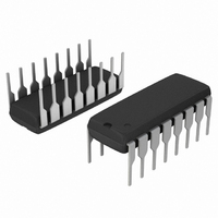
MC14526BCPG ON Semiconductor, MC14526BCPG Datasheet - Page 7

MC14526BCPG
Manufacturer Part Number
MC14526BCPG
Description
IC COUNTER BINARY 4BIT 16-DIP
Manufacturer
ON Semiconductor
Series
4000Br
Specifications of MC14526BCPG
Logic Type
Binary Counter, Decade
Direction
Down
Number Of Elements
1
Number Of Bits Per Element
4
Reset
Asynchronous
Count Rate
6.6MHz
Trigger Type
Positive, Negative
Voltage - Supply
3 V ~ 18 V
Operating Temperature
-55°C ~ 125°C
Mounting Type
Through Hole
Package / Case
16-DIP (0.300", 7.62mm)
Counter Type
Binary
Counting Sequence
Down
Number Of Circuits
1
Logic Family
14526
Propagation Delay Time
1100 ns, 450 ns, 320 ns
Supply Voltage (max)
18 V
Maximum Operating Temperature
+ 125 C
Minimum Operating Temperature
- 55 C
Function
Counter/Divider
Mounting Style
Through Hole
Operating Supply Voltage
3 V to 18 V
Circuit Type
Low-Power Schottky
Current, Supply
600 μA
Function Type
4-Bits, Down
Logic Function
Counter
Package Type
PDIP-16
Special Features
Binary
Temperature, Operating, Range
-55 to +125 °C
Voltage, Supply
3 to 18 VDC
Lead Free Status / RoHS Status
Lead free / RoHS Compliant
Timing
-
Lead Free Status / Rohs Status
Lead free / RoHS Compliant
Other names
MC14526BCPG
MC14526BCPGOS
MC14526BCPGOS
Available stocks
Company
Part Number
Manufacturer
Quantity
Price
Part Number:
MC14526BCPG
Manufacturer:
ON/安森美
Quantity:
20 000
Divide−By−N, Single Stage
inputs (P0, P1, P2, and P3) and reset is taken high
asynchronously. A zero is forced into the master and slave
of each bit and, at the same time, the “0” output goes high.
Because Preset Enable is tied to the “0” output, preset is
enabled. Reset must be released while the Clock is high so
the slaves of each bit may receive N before the Clock goes
low. When the Clock goes low and Reset is low, the “0”
output goes low (if P0 through P3 are unequal to zero).
Clock. When the counter reaches the zero state, an output
pulse occurs on “0” which presets N. The propagation delays
from the Clock’s rising and falling edges to the “0” output’s
rising and falling edges are about equal, making the “0”
output pulse approximately equal to that of the Clock pulse.
this pin is taken high, decrementing is inhibited.
Figure 11 shows a single stage divide−by−N application.
To initialize counting a number, N is set on the parallel
The counter downcounts with each rising edge of the
The Inhibit pin may be used to stop pulse counting. When
INHIBIT
CLOCK
RESET
CF
PE
13
10
3
4
6
P0
5
D
C
T
PE
R
Q
Q0
V
7
DD
APPLICATIONS INFORMATION
MC14526B LOGIC DIAGRAM
P1
(Binary Down Counter)
11
D
C
T
http://onsemi.com
PE Q
R Q
MC14526B
Q1
7
9
V
Cascaded, Presettable Divide−By−N
Reset high loads N. Only the first stage’s Reset pin (least
significant counter) must be taken high to cause the preset
for all stages, but all pins could be tied together, as shown.
is latched in a high state. Reset must be released while Clock
is high and time allowed for Preset Enable to load N into all
stages before Clock goes low.
be allowed for the zero digits to propagate a Cascade
Feedback to the first non−zero stage. Worst case is from the
most significant bit (M.S.B.) to the L.S.B., when the L.S.B.
is equal to one (i.e. N = 1).
each rising edge of Clock. When any stage reaches zero and
the leading stages (more significant bits) are zero, the “0”
output goes high and feeds back to the preceding stage.
When all stages are zero, the Preset Enable automatically
loads N while the Clock is high and the cycle is renewed.
DD
Figure 12 shows a three stage cascade application. Taking
When the first stage’s Reset pin goes high, the “0” output
When Preset Enable is high and Clock is low, time must
After N is loaded, each stage counts down to zero with
P2
14
D
C
T
PE Q
R Q
Q2
15
P3
2
D
C
T
PE Q
R Q
12
Q3
1
0"


