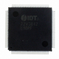
IDT72V3642L10PF IDT, Integrated Device Technology Inc, IDT72V3642L10PF Datasheet - Page 11

IDT72V3642L10PF
Manufacturer Part Number
IDT72V3642L10PF
Description
IC FIFO SYNC 3.3V CMOS 120-TQFP
Manufacturer
IDT, Integrated Device Technology Inc
Series
72Vr
Datasheet
1.IDT72V3642L10PF.pdf
(29 pages)
Specifications of IDT72V3642L10PF
Function
Synchronous
Memory Size
72M (1M x 72)
Data Rate
100MHz
Access Time
10ns
Voltage - Supply
3 V ~ 3.6 V
Operating Temperature
0°C ~ 70°C
Mounting Type
Surface Mount
Package / Case
120-TQFP, 120-VQFP
Lead Free Status / RoHS Status
Contains lead / RoHS non-compliant
Other names
72V3642L10PF
800-1534
800-1534
Available stocks
Company
Part Number
Manufacturer
Quantity
Price
Company:
Part Number:
IDT72V3642L10PF
Manufacturer:
IDT, Integrated Device Technology Inc
Quantity:
10 000
Company:
Part Number:
IDT72V3642L10PF8
Manufacturer:
IDT, Integrated Device Technology Inc
Quantity:
10 000
FIFO WRITE/READ OPERATION
Select (CSA) and port A Write/Read select (W/RA). The A0-A35 outputs are
in the high-impedance state when either CSA or W/RA is HIGH. The A0-A35
outputs are active when both CSA and W/RA are LOW.
transition of CLKA when CSA is LOW, W/RA is HIGH, ENA is HIGH , MBA is
LOW, and FFA/IRA is HIGH. Data is read from FIFO2 to the A0-A35 outputs
by a LOW-to-HIGH transition of CLKA when CSA is LOW, W/RA is LOW, ENA
is HIGH, MBA is LOW, and EFA/ORA is HIGH (see Table 2). FIFO reads and
writes on port A are independent of any concurrent port B operation. Write and
Read cycle timing diagrams for Port A can be found in Figure 4 and 7.
that the port B Write/Read select (W/RB) is the inverse of the port A Write/Read
select (W/RA). The state of the port B data (B0-B35) outputs is controlled by the
port B Chip Select (CSB) and port B Write/Read select (W/RB). The B0-B35
outputs are in the high-impedance state when either CSB is HIGH or W/RB
is LOW. The B0-B35 outputs are active when CSB is LOW and W/RB is HIGH.
transition of CLKB when CSB is LOW, W/RB is LOW, ENB is HIGH, MBB is
LOW, and FFB/IRB is HIGH. Data is read from FIFO1 to the B0-B35 outputs
by a LOW-to-HIGH transition of CLKB when CSB is LOW, W/RB is HIGH, ENB
is HIGH, MBB is LOW, and EFB/ORB is HIGH (see Table 3) . FIFO reads and
writes on port B are independent of any concurrent port A operation. Write and
Read cycle timing diagrams for Port B can be found in Figure 5 and 6.
Selects and Write/Read selects are only for enabling write and read operations
TABLE 2 — PORT A ENABLE FUNCTION TABLE
TABLE 3 — PORT B ENABLE FUNCTION TABLE
IDT72V3622/72V3632/72V3642 CMOS 3.3V SyncBiFIFO
256 x 36 x 2, 512 x 36 x 2, 1,024 x 36 x 2
CSA
CSB
The state of the port A data (A0-A35) outputs is controlled by port A Chip
Data is loaded into FIFO1 from the A0-A35 inputs on a LOW-to-HIGH
The port B control signals are identical to those of port A with the exception
Data is loaded into FIFO2 from the B0-B35 inputs on a LOW-to-HIGH
The setup and hold time constraints to the port Clocks for the port Chip
H
L
L
L
L
L
L
L
H
L
L
L
L
L
L
L
W/RB
W/RA
H
H
H
X
L
L
L
L
H
H
H
H
X
L
L
L
ENA
ENB
H
H
H
H
X
L
L
L
H
H
H
H
X
L
L
L
MBB
MBA
H
H
H
X
X
L
L
L
H
H
H
X
X
L
L
L
CLKB
CLKA
X
X
↑
↑
X
↑
X
↑
X
X
↑
↑
X
↑
X
↑
TM
11
Data B (B0-B35) I/O
Data A (A0-A35) I/O
and are not related to high-impedance control of the data outputs. If a port enable
is LOW during a clock cycle, the port’s Chip Select and Write/Read select may
change states during the setup and hold time window of the cycle.
the next word written is automatically sent to the FIFO’s output register by the
LOW-to-HIGH transition of the port clock that sets the Output Ready flag HIGH.
When the Output Ready flag is HIGH, subsequent data is clocked to the output
registers only when a read is selected using the port’s Chip Select, Write/Read
select, Enable, and Mailbox select.
the Empty Flag to change state on the second LOW-to-HIGH transition of the
Read Clock. The data word will not be automatically sent to the output register.
Instead, data residing in the FIFO's memory array is clocked to the output
register only when a read is selected using the port’s Chip Select, Write/Read
select, Enable, and Mailbox select.
SYNCHRONIZED FIFO FLAGS
stages. This is done to improve flag signal reliability by reducing the probability
of metastable events when CLKA and CLKB operate asynchronously to one
another. EFA/ORA, AEA, FFA/IRA, and AFA are synchronized to CLKA.
EFB/ORB, AEB, FFB/IRB, and AFB are synchronized to CLKB. Tables
4 and 5 show the relationship of each port flag to FIFO1 and FIFO2.
EMPTY/OUTPUT READY FLAGS (EFA/ORA, EFB/ORB)
(ORA, ORB) function is selected. When the Output Ready flag is HIGH,
High-Impedance
High-Impedance
When operating the FIFO in FWFT mode and the Output Ready flag is LOW,
When operating the FIFO in IDT Standard mode, the first word will cause
These are dual purpose flags. In the FWFT mode, the Output Ready
Each FIFO is synchronized to its port clock through at least two flip-flop
Output
Output
Output
Output
Output
Output
Output
Output
Input
Input
Input
Input
Input
Input
COMMERCIAL TEMPERATURE RANGE
Mail2 read (set MBF2 HIGH)
Mail1 read (set MBF1 HIGH)
Port Function
Port Function
FIFO1 write
FIFO2 read
Mail1 write
FIFO2 write
FIFO1 read
Mail2 write
None
None
None
None
None
None
None
None


